3 dsp i/o description, 1 multiplexed pins, 2 termination requirements – Cirrus Logic CS4970x4 User Manual
Page 8: 3 pads, 4 application code security, 5 characteristics and specifications, 1 absolute maximum ratings

CS4970x4 Data Sheet
32-bit High Definition Audio Decoder DSP Family
DS752F1
8
through master boot from an external FLASH or through host control. A built-in crystal oscillator circuit with a
buffered output is provided. The buffered output frequency ratio is selectable between 1:1 (default) or 2:1.
4.3 DSP I/O Description
4.3.1 Multiplexed Pins
Many of the CS4970x4 pins are multi-functional. For details on pin functionality please refer to the CS4970x4
System Designer’s Guide.
4.3.2 Termination Requirements
Open-drain pins on the CS4970x4 must be pulled high for proper operation. Please refer to the CS4970x4
System Designer’s Guide to identify which pins are open-drain and what value of pull-up resistor is required for
proper operation.
Mode select pins on the CS4970x4 are used to select the boot mode upon the rising edge of reset. A detailed
explanation of termination requirements for each communication mode select pin can be found in the
CS4970x4 System Designer’s Guide.
4.3.3 Pads
The CS4970x4 I/O operates from the 3.3 V supply and is tolerant within 5 V.
4.4 Application Code Security
The external program code may be encrypted by the programmer to protect any intellectual property it may
contain. A secret, customer-specific key is used to encrypt the program code that is to be stored external to the
device.
5 Characteristics and Specifications
Note:
All data sheet minimum and maximum timing parameters are guaranteed over the rated voltage
and temperature. All data sheet typical parameters are measured under the following conditions:
T = 25 °C, C
L
= 20 pF, VDD = 1.8 V, VDDA = VDDIO = 3.3 V, GNDD = GNDIO = GNDA = 0 V.
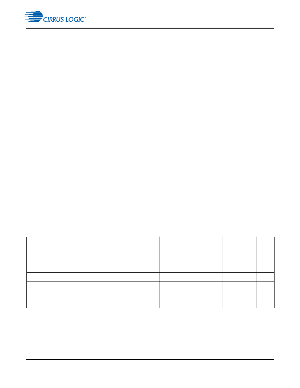
5.1 Absolute Maximum Ratings
(GNDD = GNDIO = GNDA = 0 V; all voltages with respect to 0 V)
CAUTION: Operation at or beyond these limits may result in permanent damage to the device. Normal operation is
not guaranteed at these extremes.
Parameter
Symbol
Min
Max
Unit
DC power supplies:
Core supply
PLL supply
I/O supply
|VDDA – VDDIO|
VDD
VDDA
VDDIO
–0.3
–0.3
–0.3
—
2.0
3.6
3.6
0.3
V
V
V
V
Input pin current, any pin except supplies
I
in
—
+/- 10
mA
Input voltage on PLL_REF_RES
V
filt
-0.3
3.6
V
Input voltage on I/O pins
V
inio
-0.3
5.0
V
Storage temperature
T
stg
-65
150
°C
