Figure 2. system block diagram and signal flow, Cdb 4382 – Cirrus Logic CDB4382 User Manual
Page 6
CDB
4382
6
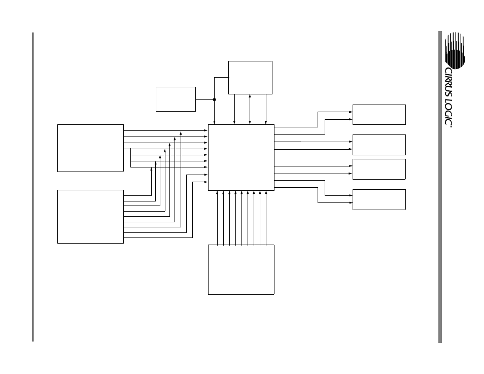
Figure 2. System Block Diagram and Signal Flow
CS4382
DSD Inputs
DSD1A
DSD1B
DSD2A
DSD2B
DSD3A
DSD3B
DSD4A
DSD4B
DSD_CLK
PCM Inputs
8414 Digital
Audio Receiver
MCLK
SCLK1
LRCK1
SDATA1
SDATA2
SDATA3
SDATA4
SCLK2
LRCK2
Control Port
Reset
Circuit
Channels 1A & 1B
Channels 2A & 2B
Channels 3A & 3B
Channels 4A & 4B
Outputs and Mute
Outputs and Mute
Outputs and Mute
Outputs and Mute
Figure 3
Figure 6
Figure 7
Figure 5
Figure 4
Figure 8
Figure 9
Figure 10
Figure 11
See also other documents in the category Cirrus Logic Hardware:
- CobraNet (147 pages)
- CS4961xx (54 pages)
- CS150x (8 pages)
- CS1601 (2 pages)
- CS1501 (16 pages)
- CS1601 (16 pages)
- CS1610 (16 pages)
- CRD1610-8W (24 pages)
- CRD1611-8W (25 pages)
- CDB1610-8W (21 pages)
- CS1610A (18 pages)
- CDB1611-8W (21 pages)
- CDB1610A-8W (21 pages)
- CDB1611A-8W (21 pages)
- CRD1610A-8W (24 pages)
- CRD1611A-8W (25 pages)
- CS1615 (16 pages)
- AN403 (15 pages)
- AN401 (14 pages)
- AN400 (15 pages)
- AN375 (27 pages)
- AN376 (9 pages)
- CRD1615-8W (22 pages)
- CRD1616-8W (23 pages)
- AN402 (14 pages)
- AN404 (15 pages)
- CRD1615A-8W (21 pages)
- CS1615A (16 pages)
- CS1630 (56 pages)
- AN374 (35 pages)
- AN368 (80 pages)
- CRD1630-10W (24 pages)
- CRD1631-10W (25 pages)
- CS1680 (16 pages)
- AN405 (13 pages)
- AN379 (31 pages)
- CRD1680-7W (31 pages)
- AN335 (10 pages)
- AN334 (6 pages)
- AN312 (14 pages)
- AN Integrating CobraNet into Audio Products (16 pages)
- CobraNet Audio Routing Primer (9 pages)
- Bundle Assignments in CobraNet Systems (3 pages)
- CS2300-01 (3 pages)
- CS2000-CP (38 pages)