Board connections and settings, Table 1. system connections, Table 2. cdb4354 jumper pin block settings – Cirrus Logic CDB4354 User Manual
Page 5: Table 3. led information, Se use, Table 2
DS895DB1
5
CDB4354
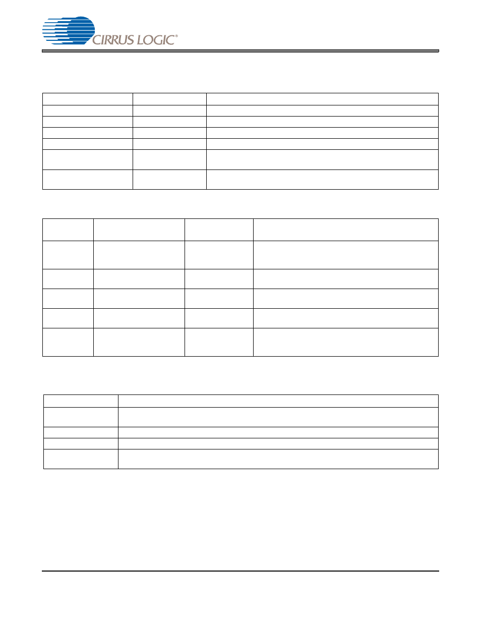
2. BOARD CONNECTIONS AND SETTINGS
Board connections and settings are shown in
and
Table 1. System Connections
Table 2. CDB4354 Jumper Pin Block Settings
Table 3. LED Information
Note: All settings denoted by an asterisk (*) are the Factory Default Settings.
CONNECTOR
INPUT/OUTPUT
SIGNAL PRESENT
+5 V - J2
Input
+3.3 V power for the evaluation board
GND - J1
Input
Ground connection from power supply
S/PDIF INPUT - J16
Input
Digital audio interface input via coaxial cable
S/PDIF INPUT - OPT1
Input
Digital audio interface input via optical cable
Serial Audio Header Pin
Block - J6
Input
Input for master, serial, left/right clocks and serial data (MCLK, SCLK,
LRCK, and SDIN) - direct to CS4354
AOUTA - J7
AOUTB - J8
Output
RCA line-level analog outputs
JUMPER PIN
BLOCK
PURPOSE
POSITION
FUNCTION SELECTED
J12
Selects source of voltage
for the VL supply
pins [1, 2] shunted
*pins [2,3] shunted
not shunted
Voltage source is +5 V
Voltage source is +3.3 V
Voltage source is pin 2 of J12
J4
Current measure for VL
*shunted
not shunted
When shunt is removed, the voltage can be measured
across a fixed resistance R2 to determine current.
J5
Current measure for VA
*shunted
not shunted
When shunt is removed, the voltage can be measured
across a fixed resistance R3 to determine current.
J9
CS8416 Manual Reset
shunted
*not shunted
CS8416
is held in reset as long as J9 is shunted
CS8416 uses the on-board automatic reset
J3
CS4354 De-emphasis and
Internal Serial Clock Mode
Select
pins [1, 2] shunted
*pins [2, 3] shunted
not shunted
Internal Serial Clock Mode, De-emphasis enabled
External Serial Clock Mode, De-emphasis disabled
Internal Serial Clock Mode, De-emphasis disabled
LED
FUNCTION
+3.3V - D1
LED is illuminated when the +3.3 V supply is on (+3.3V is derived from the +5V supply by an on-board
regulator)
+5V - D2
LED is illuminated when the +5 V supply is on
VL - D4
LED is illuminated when the VL supply is on (either by the onboard +3.3 V, +5 V or external supply)
S/PDIF - D10
LED is illuminated when the CS8416 reports a Receiver Error. See the CS8416 datasheet for a full
description of the error reporting functionality.