Cirrus Logic AN306 User Manual
An306, Simplifying system design using the cs4350 pll dac, Introduction
Copyright
Cirrus Logic, Inc. 2009
(All Rights Reserved)
Simplifying System Design Using the CS4350 PLL DAC
1. INTRODUCTION
Typical Digital to Analog Converters (DACs) require a high-speed Master Clock to clock their digital filters and mod-
ulators, as well as some portions of their discrete time analog circuitry. This Master Clock (or system clock) is typi-
cally required to be synchronous to the left-right (frame or word) clock (LRCK) in order to maintain sample alignment
in the digital filters, state machines, modulator and discrete time analog sections.
below shows an example
of a typical DAC clocked by an external Master Clock. The clock is applied to the MCLK pin and then distributed to
any internal logic that requires it.
As an alternative, PLL DACs are designed to derive their internal synchronous Master Clock from some other ex-
ternal source. This source could be any clock, but in practice it is commonly a video clock (27 MHz) or one of the
slower SCLK or LRCK signals which are mandatory for typical PCM audio interfaces (See AN282 “The 2-Channel
Serial Audio Interface: A Tutorial”). In practice, the CS4350 PLL DAC generates its Master Clock from the input left-
right clock.
shows the CS4350 PLL DAC architecture; from the input LRCK signal, the internal PLL derives
the Master Clock signal that is used to drive the internal system timing.
The internal Master Clock generation of a PLL DAC yields inherent benefits that simplify the design of audio sys-
tems. The CS4350’s unique implementation of the feature takes the concept a step further to provide an even great-
er degree of design simplicity, flexibility, and performance.
PCM
Serial
Interface
Serial Data Input
Right
Channel
Output
Left
Channel
Output
Left-Right Clock
Master Clock
Interpolation
Filter with
Volume
Control
Interpolation
Filter with
Volume
Control
Multibit
ΔΣ
Modulator
Multibit
ΔΣ
Modulator
Amp
+
Filter
Amp
+
Filter
DAC
DAC
Serial Clock
Figure 1. Typical DAC Architecture with Master Clock Input
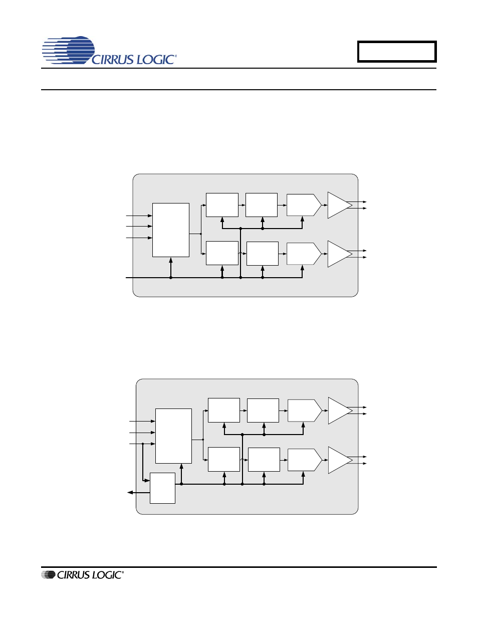
PCM
Serial
Interface
Serial Data Input
Right
Channel
Output
Left
Channel
Output
Left-Right Clock
Recovered MCLK
Phase
Locked
Loop
Interpolation
Filter with
Volume
Control
Interpolation
Filter with
Volume
Control
Multibit
ΔΣ
Modulator
Multibit
ΔΣ
Modulator
Amp
+
Filter
Amp
+
Filter
DAC
DAC
Serial Clock
Internal MCLK
Figure 2. CS4350 PLL DAC Architecture
AN306
AUG '09
AN306REV1