Cirrus Logic CRD42L52 User Manual
Crd42l52, Reference design board (crd42l52) features, Peripheral driver board (cdb42ldb1) features
Copyright
© Cirrus Logic, Inc. 2008
(All Rights Reserved)
Reference Design and Peripheral Driver Board for CS42L52
Reference Design Board (CRD42L52)
Features
Ultra-Small Layout
Stake Header for External System Connections
1/8” Stereo Input Allows up to 2 Vrms Signals
1/8” Stereo Headphone Output Jack
Built-in Switch Control for CS42L52 SPKR/HP
Pin
Stereo Full Bridge Speaker Output Terminal
Complies with FCC class B and CISPR 22
Standards for Radiated Emissions
Peripheral Driver Board (CDB42LDB1)
Features
Multiple Power Supply Options
–
Three AAA Battery Source
–
External Power Supply Header
S/PDIF I/O (CS8416 Receiver)
–
Optical and RCA Input Jacks
S/PDIF I/O (CS8406 Transmitter)
–
Optical and RCA Output Jacks
FlexGUI S/W Control - Windows
®
Compatible
–
Pre-Defined & User Configurable Scripts
Description
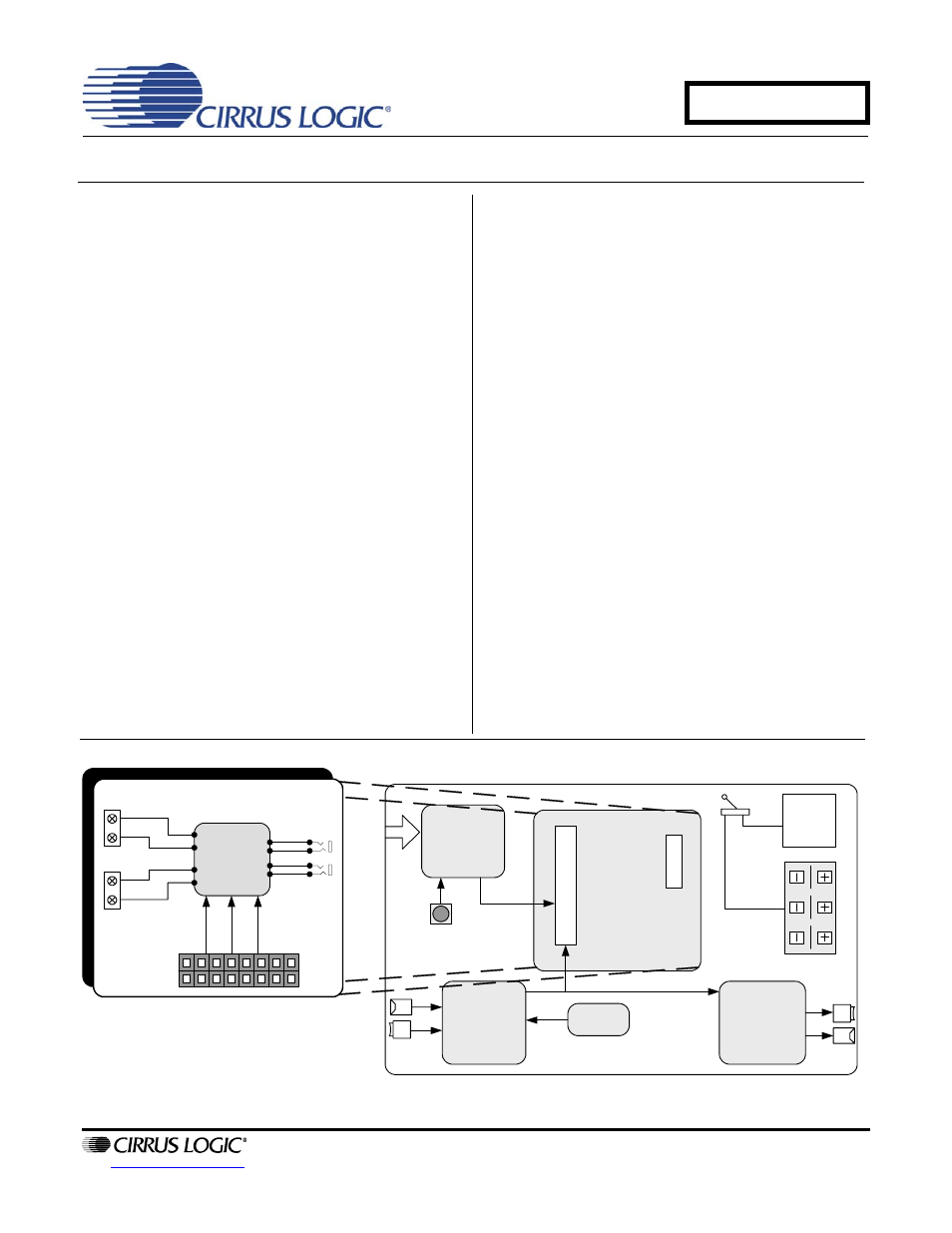
In addition to providing a reference for an ultra small lay-
out design, the purpose of the CRD42L52 is to allow a
quick and easy evaluation of the CS42L52 low power
stereo CODEC.
Two 1/8” stereo jacks on the CRD42L52 provide an in-
terface for analog line-level input and headphone-level
output connections to the CS42L52. Stereo differential
PWM speaker outputs from the CS42L52 can be moni-
tored on a pair of screw terminals on the CRD42L52.
The control port and serial audio interfaces are accessi-
ble via the I/O stake header used to attach the
CRD42L52 to the CDB42LDB1.
The CDB42LDB1 is a peripheral driver board that pro-
vides clock/data, control logic and power supply to the
CRD42L52. Digital data is transmitted and received via
S/PDIF optical and RCA connectors. The CRD42L52
can be programmed by using the Windows Compatible
FlexGUI software provided. Power is derived either
from three AAA batteries or from an external supply on
the CDB42LDB1 driver board and is routed to the
CRD42L52 via the I/O stake header.
ORDERING INFORMATION
CRD42L52
Reference Design
CDB42LDB1
Driver Board
CS42L52
Left
Right
+
-
+
-
I²C
Control
Port
SAI
Power
Supply
Line
Input
Headphone
Output
Speaker
J5
Microcontroller
S/PDIF Rx
CS8416
S/PDIF Tx
CS8406
12.288 MHz
External
Power
S/PDIF
Input
S/PDIF
Output
J4
J3
USB
I/O Header
AAA Battery
Clip
MCLK
Serial Audio Interface
I²C Control Port
Interface
Micro Reset
Pushbutton
CRD
Placeholder
CRD42L52
CDB42LDB1
APRIL '08
DS680RD1
CRD42L52
Document Outline
- Table of Contents
- List of Figures
- List of Tables
- 1. System Overview
- 2. Quick-Start Guide
- 3. Configuration Options
- 4. Software Mode Control
- 5. Performance Plots
- Figure 9. Dynamic Range - Line In to S/PDIF Out
- Figure 10. Freq. Resp. - Line In to S/PDIF Out
- Figure 11. THD + N - Line In to S/PDIF Out
- Figure 12. FFT - S/PDIF In to HP Out @ 0 dBFS
- Figure 13. FFT - S/PDIF In to HP Out @ -60 dBFS
- Figure 14. Dynamic Range - S/PDIF In to HP Out
- Figure 15. Freq. Resp. - S/PDIF In to HP Out
- Figure 16. THD + N - S/PDIF In to HP Out
- Figure 17. Freq. Resp. - S/PDIF In to Spkr. Out
- Figure 18. Dynamic Range - Line In to HP Out (Dig. LB)
- Figure 19. THD + N - Line In to HP Out (Dig. LB)
- 6. System Connections & Interface
- 7. CRD42L52 Schematics
- 8. CDB42LDB1 Schematics
- 9. CRD42L52 Layout
- 10. CDB42LDB1 Layout
- 11. Revision History