Cirrus Logic CDB4271 User Manual
Features, Description, Cs4271
1
Copyright
Cirrus Logic, Inc. 2003
(All Rights Reserved)
Cirrus Logic, Inc.
www.cirrus.com
CDB4271
Evaluation Board For CS4271
Features
Single-ended inputs
CS8406 S/PDIF digital audio transmitter
CS8416 S/PDIF digital audio receiver
Header for optional external configuration of
CS4271
Header for external DSP serial audio I/O
3.3V to 5.0V Logic Interface
Demonstrates recommended layout and
grounding arrangements
Microsoft Windows
®
compatible software
interface to configure CS4271 and inter-
board connections
ORDERING INFORMATION
CDB4271
Evaluation Board
Description
The CDB4271 demonstration board is an excellent
means for evaluating the CS4271 stereo CODEC. Eval-
uation requires an analog/digital signal source and
analyzer, and power supplies. Optionally, a Windows
®
PC compatible computer may be used to evaluate the
CS4271 in control port mode.
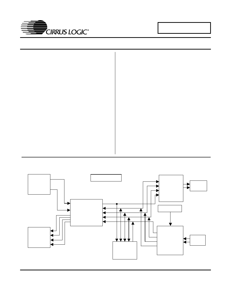
System timing can be provided by the CS4271, by the
CS8416 phase-locked to its S/PDIF input, by an I/O
stake header or by an on-board oscillator. RCA phono
jacks are provided for the CS4271 analog outputs and in-
puts. Digital data I/O is available via RCA phono or
optical connectors to the CS8416 and CS8406.
Microsoft Windows
®
software provides a GUI to make
configuration of the board easy. The software communi-
cates through the PC’s parallel port to configure the
hardware so that all features of the CS4271 can be eval-
uated. The evaluation board may also be configured to
accept external timing and data signals for operation in a
user application during system development.
I
CS4271
Single-Ended
Analog Inputs
Control Port
CS8406
S/PDIF
Transmitter
CS8416
S/PDIF
Receiver
I/O
Header for
Clocks &
Data
Oscillator
S/PDIF
Output
S/PDIF
Input
MCLK
LRCK
SCLK
SDIN
SDOUT
Differential to
Single-Ended
Analog
Outputs
SEPT ‘03
DS592DB2
Document Outline
- CDB4271
- Features
- Description
- 1. System Overview
- 2. Initial Board Setup
- 3. CDB427X.exe User's Guide
- 4. Block Diagram
- 5. Schematics and Layout
- Figure 6. Hierarchy, Schematic Sheet 1
- Figure 7. CS4271 Schematic Sheet 2
- Figure 8. Analog Input, Schematic Sheet 3
- Figure 9. Analog Output, Schematic Sheet 4
- Figure 10. CS8416 S/PDIF Receiver, Schematic Sheet 5
- Figure 11. CS8406 S/PDIF Transmitter, Schematic Sheet 6
- Figure 12. Board Setup, Schematic Sheet 7
- Figure 13. PCM Header, Schematic Sheet 8
- Figure 14. Control Port, Schematic Sheet 9
- Figure 15. Power, Schematic Sheet 10
- Figure 16 . Component Placement and Reference Designators
- Figure 17 . Top Layer
- Figure 18 . Bottom Layer