Cirrus Logic CS42516 User Manual
Features, General description, Six 24-bit d/a, two 24-bit a/d converters
Copyright
Cirrus Logic, Inc. 2014
(All Rights Reserved)
110 dB, 192-kHz 6-Ch CODEC with S/PDIF Receiver
Features
Six 24-bit D/A, two 24-bit A/D Converters
110 dB DAC / 114 dB ADC Dynamic Range
-100 dB THD+N
System Sampling Rates up to 192 kHz
S/PDIF Receiver Compatible with EIAJ
CP1201 and IEC-60958
Recovered S/PDIF Clock or System Clock
Selection
8:2 S/PDIF Input MUX
ADC High-Pass Filter for DC Offset Calibration
Expandable ADC Channels and One-Line
Mode Support
Digital Output Volume Control with Soft Ramp
Digital ±15 dB Input Gain Adjust for ADC
Differential Analog Architecture
Supports Logic Levels between 1.8 V and 5 V
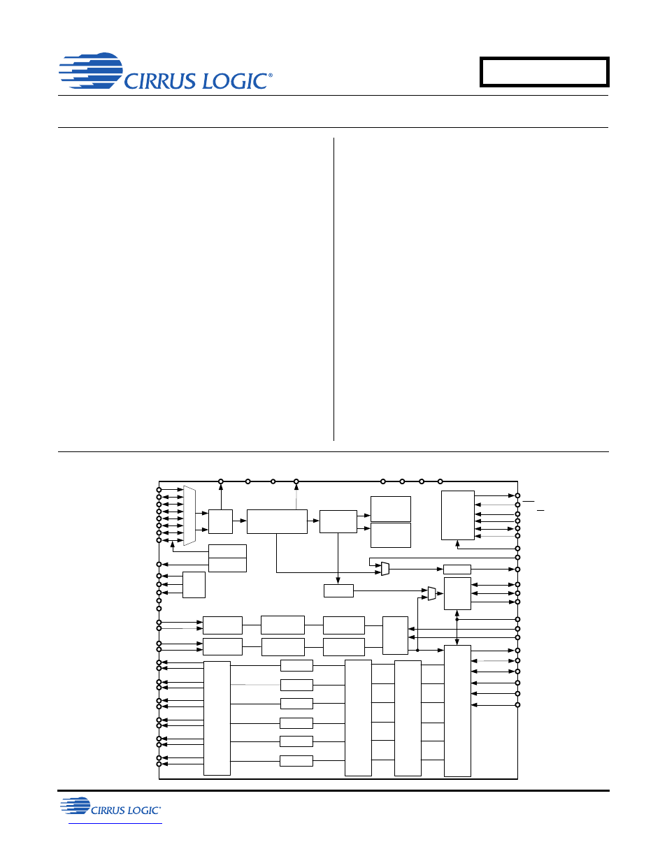
General Description
The CS42516 provides two analog-to-digital and six
digital-to-analog delta-sigma converters, as well as an
integrated S/PDIF receiver.
The CS42516 integrated S/PDIF receiver supports up
to eight inputs, clock recovery circuitry and format auto-
detection. The internal stereo ADC is capable of inde-
pendent channel gain control for single-ended or
differential analog inputs. All six channels of DAC pro-
vide digital volume control and differential analog
outputs. The general-purpose outputs may be driven
high or low, or mapped to a variety of DAC mute con-
trols or ADC overflow indicators.
The CS42516 is ideal for audio systems requiring wide
dynamic range, negligible distortion and low noise, such
as A/V receivers, DVD receivers, and digital speakers.
The CS42516 is available in a 64-pin LQFP package in
Commercial (-10° to +70° C) grades. The CDB42518
Customer Demonstration board is also available for de-
vice evaluation. Refer to
RST
RXP0
RXP1/GPO1
AD0/CS
SCL/CCLK
SDA/CDOUT
AD1/CDIN
VLC
AOUTA1+
AOUTA1-
AOUTB1+
AOUTA3+
AOUTA3-
AOUTA2-
AOUTB2-
AOUTA2+
AOUTB2+
AOUTB1-
AOUTB3+
AOUTB3-
AINL+
AINL-
AINR+
AINR-
FILT+
REFGND
VQ
Ref
ADC#1
ADC#2
Digital Filter
Digital Filter
Gain & Clip
Gain & Clip
CX_SCLK
CX_LRCK
CX_SDIN3
CX_SDIN2
CX_SDIN1
DGND VD
LPFLT
TXP
INT
Rx
Clock/Data
Recovery
S/PDIF
Decoder
Control
Port
DAC#1
DAC#2
DAC#3
DAC#4
DAC#5
DAC#6
D
igi
ta
l Filte
r
V
ol
ume
C
ontr
ol
DGND
RXP2/GPO2
RXP3/GPO3
RXP4/GPO4
RXP5/GPO5
RXP6/GPO6
RXP7/GPO7
VD
MUTEC
GPO
An
al
og
F
ilt
er
VARX AGND
AGND
VA
CODEC
Serial
Port
CX_SDOUT
ADCIN1
ADCIN2
VLS
SAI_LRCK
SAI_SCLK
SAI_SDOUT
OMCK
RMCK
Serial
Audio
Interface
Port
ADC
Serial
Data
Internal MCLK
Mult/Div
DEM
C&U Bit
Data Buffer
Format
Detector
MUTE
MAR '14
DS583F2
CS42516
Document Outline
- 1. Characteristics and Specifications
- Specified Operating Conditions
- Absolute Maximum Ratings
- Analog Input Characteristics
- A/D Digital Filter Characteristics
- Analog Output Characteristics
- D/A Digital Filter Characteristics
- Switching Characteristics
- Switching Characteristics - Control Port - I²C™ Format
- Switching Characteristics - Control Port - SPI™ Format
- DC Electrical Characteristics
- Digital Interface Characteristics
- 2. Pin Descriptions
- 3. Typical Connection Diagram
- 4. Applications
- 4.1 Overview
- 4.2 Analog Inputs
- 4.3 Analog Outputs
- 4.4 S/PDIF Receiver
- 4.5 Clock Generation
- 4.6 Digital Interfaces
- 4.7 Control Port Description and Timing
- 4.8 Interrupts
- 4.9 Reset and Power-Up
- 4.10 Power Supply, Grounding, and PCB Layout
- 5. Register Quick Reference
- 6. Register Description
- Table 5. DAC De-Emphasis
- Table 6. Receiver De-Emphasis
- Table 7. Digital Interface Formats
- Table 8. ADC One-Line Mode
- Table 9. DAC One-Line Mode
- Table 10. RMCK Divider Settings
- Table 11. OMCK Frequency Settings
- Table 12. Master Clock Source Select
- Table 13. AES Format Detection
- Table 14. Receiver Clock Frequency Detection
- Table 15. Example Digital Volume Settings
- Table 16. ATAPI Decode
- Table 17. Example ADC Input Gain Settings
- Table 18. TXP Output Selection
- Table 19. Receiver Input Selection
- Table 20. Auxiliary Data Width Selection
- 7. Parameter Definitions
- 8. Appendix A: External Filters
- 9. Appendix B: S/PDIF Receiver
- 10. Appendix C: PLL Filter
- 11. Appendix D: External AES3-S/PDIF-IEC60958 Receiver Components
- 12. Appendix E: ADC Filter Plots
- Figure 34. Single-Speed Mode Stopband Rejection
- Figure 35. Single-Speed Mode Transition Band
- Figure 36. Single-Speed Mode Transition Band (Detail)
- Figure 37. Single-Speed Mode Passband Ripple
- Figure 38. Double-Speed Mode Stopband Rejection
- Figure 39. Double-Speed Mode Transition Band
- Figure 40. Double-Speed Mode Transition Band (Detail)
- Figure 41. Double-Speed Mode Passband Ripple
- Figure 42. Quad-Speed Mode Stopband Rejection
- Figure 43. Quad-Speed Mode Transition Band
- Figure 44. Quad-Speed Mode Transition Band (Detail)
- Figure 45. Quad-Speed Mode Passband Ripple
- 13. Appendix F: DAC Filter Plots
- Figure 46. Single-Speed (fast) Stopband Rejection
- Figure 47. Single-Speed (fast) Transition Band
- Figure 48. Single-Speed (fast) Transition Band (detail)
- Figure 49. Single-Speed (fast) Passband Ripple
- Figure 50. Single-Speed (slow) Stopband Rejection
- Figure 51. Single-Speed (slow) Transition Band
- Figure 52. Single-Speed (slow) Transition Band (detail)
- Figure 53. Single-Speed (slow) Passband Ripple
- Figure 54. Double-Speed (fast) Stopband Rejection
- Figure 55. Double-Speed (fast) Transition Band
- Figure 56. Double-Speed (fast) Transition Band (detail)
- Figure 57. Double-Speed (fast) Passband Ripple
- Figure 58. Double-Speed (slow) Stopband Rejection
- Figure 59. Double-Speed (slow) Transition Band
- Figure 60. Double-Speed (slow) Transition Band (detail)
- Figure 61. Double-Speed (slow) Passband Ripple
- Figure 62. Quad-Speed (fast) Stopband Rejection
- Figure 63. Quad-Speed (fast) Transition Band
- Figure 64. Quad-Speed (fast) Transition Band (detail)
- Figure 65. Quad-Speed (fast) Passband Ripple
- Figure 66. Quad-Speed (slow) Stopband Rejection
- Figure 67. Quad-Speed (slow) Transition Band
- Figure 68. Quad-Speed (slow) Transition Band (detail)
- Figure 69. Quad-Speed (slow) Passband Ripple
- 14. Package Dimensions
- 15. Ordering Information
- 16. References
- 17. Revision History