Figure 2. multiple-feedback low-pass filter, Design steps, Figure 3. differential input circuit – Cirrus Logic AN048 User Manual
Page 2: An48
AN48
2
2. Design Steps
Step 1: Determine the required pass band gain,
H
o
. The circuit parameters require that the magni-
tude of H
o
be greater than or equal to one. H
o
is
also negative due to the inverting op-amp configu-
ration.
Step 2: Determine the minimum input impedance.
Step 3: Select the desired filter type, Butterworth,
Bessel, etc. and the corner frequency, F
c
, for the fi-
nal design. The filter response and corner frequen-
cy determine the pass band phase and amplitude
response. The filter type determines the pole-loca-
tions and therefore alpha and beta. Table 1 lists
the normalized pole locations for several filter
types.
Table 1: Normalized Pole Locations
Step 4: Select convenient values for C
5
and C
2
.
Notice in Step 5 that K and H
o
must be selected
such that
is real.
Step 5: Given F
c
, H
o
, C
2
, C
5
, alpha and beta, cal-
culate R
1
, R
2
and R
3
using the following equa-
tions.
FILTER TYPE
α
β
Butterworth
0.7071
0.7071
Bessel
1.1030
0.6368
0.01 dB Chebyshev
0.6743
0.7075
0.1 dB Chebyshev
0.6104
0.7106
_
C5
R3
R1
C2
+
R4
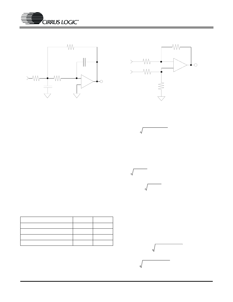
Figure 2.
Multiple-Feedback Low-Pass
Filter
_
R1
R1
R4
R4
+
Figure 3.
Differential Input Circuit
ζ
2
K 1
H
o
–
(
)
–
ζ
α
α
2
β
2
+
----------------------
=
ω
o
2
πF
c
α
2
β
2
+
=
K
C
5
C
2
-----
=
R
1
R
4
H
o
–
(
)
--------------
=
R
3
1
ω
o
C
2
ζ
ζ
2
K 1
H
o
–
(
)
–
±
[
]
--------------------------------------------------------------------
=
R
4
ζ
ζ
2
K 1
H
o
–
(
)
–
±
ω
o
C
5
⋅
-------------------------------------------------
=