6 differential analog inputs, 7 speaker outputs, 1 optional speaker output emi filter components – Cirrus Logic CRD35L01 User Manual
Page 5: Crd35l01
DS914RD2
5
CRD35L01
By adding series resistance to the input, the signal amplitude to the CS35L01 will be reduced, and will
reduce the overall system gain. The typical input impedance values of the CS35L01 can be found in the
device datasheet.
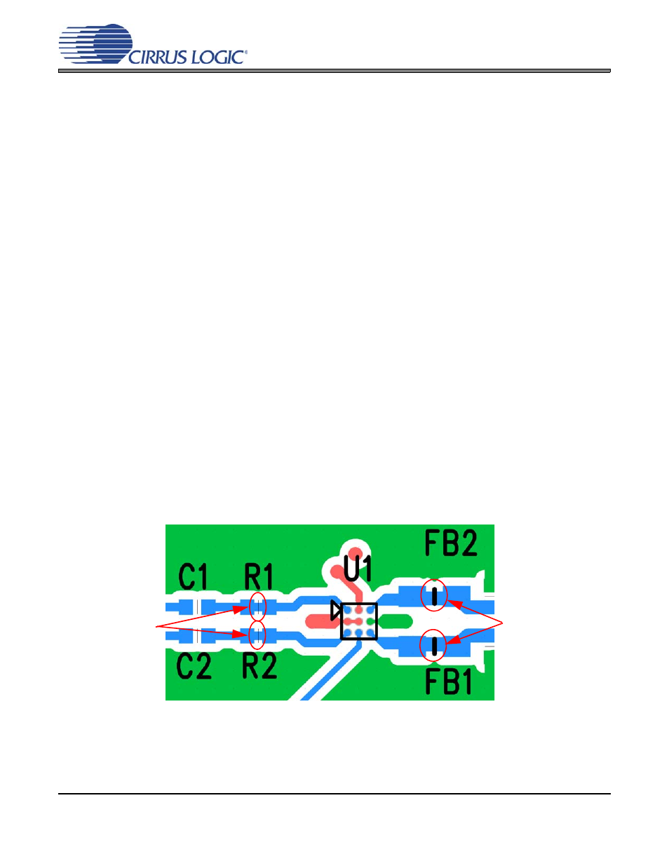
In order to use the optional gain adjustment resistors, the traces between the R1 pads and the traces be-
tween the R2 pads must be cut to break the bypass circuit, before populating R1 and R2 with the desired
resistance values. The location of these required cuts are shown in
. After the trace between the
pads has been broken, the gain adjustment resistors can be added to the board.
1.6
Differential Analog Inputs
The differential audio inputs into the CS35L01 are provided by the 3-pin header (J1) through DC blocking
capacitors (C1 and C2). The C1 and C2 capacitors allow for an analog source to connect directly to the
CS35L01 regardless of any DC bias that may be present between the analog audio source’s outputs and
CS35L01 inputs.
1.7
Speaker Outputs
The CS35L01 power outputs are configured for a full-bridge, single audio channel. The outputs are routed
through an optional EMI output filter and then presented at the J3 header (OUT- and OUT+).
1.7.1
Optional Speaker Output EMI Filter Components
As mentioned above, the CS35L01 contains optional placeholders for a series ferrite bead and shunt ca-
pacitor output filter. For most applications with very short speaker leads between the CS35L01 and the
speaker, use of these components will not be necessary. However, if there is a long signal path between
the CS35L01 and the speaker or if the system requires connecting to cables off the PCB, it is suggested
that the ferrite bead and capacitor are populated with the recommended values shown in
In order to use the optional output filter ferrite beads, the traces between the L1 pads and the traces be-
tween the L2 pads must be cut to break the bypass circuit, before populating L1 and L2 with the desired
component values. The location of these required cuts are shown in
.
Figure 1. Optional Bypass Trace Cut Locations
Cut the bypass
traces before insert-
ing the optional
input gain adjust-
ment resistors
Cut the bypass
traces before insert-
ing the optional out-
put filter ferrite
beads