Figure 13. control port timing, i·c read, 2 spi mode, Figure 14. spi write cycle – Cirrus Logic CS3318 User Manual
Page 28: Figure 13, Cs3318, Figure 13. control port timing, i²c read
28
DS693F1
CS3318
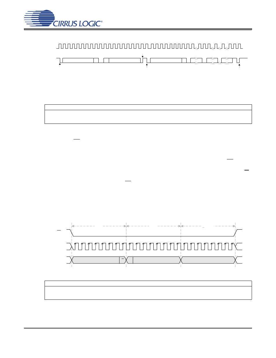
Since the read operation cannot set the MAP, an aborted write operation is used as a preamble. As shown
in
, the write operation is aborted after the acknowledge for the MAP byte by sending a stop con-
dition.
5.9.2
SPI Mode
In SPI Mode, CS is the CS3318 chip-select signal, CCLK, is the control port bit clock (input into the
CS3318 from the microcontroller), and MOSI is the input data line from the microcontroller. Data is
clocked in on the rising edge of CCLK. The default chip address in SPI Mode is 1000000b.
shows the operation of the control port in SPI Mode. To write to a register, bring CS low. The
first seven bits on MOSI form the chip address and must be either the Individual, Group 1, or Group 2 chip
address as set by their respective control port registers. The eighth bit is a read/write indicator (R/W),
which must be low to write. If the read/write indicator is set high (indicating a read operation), the CS3318
will ignore all traffic on the SPI bus until CS is brought high and then low again. The next eight bits form
the Memory Address Pointer (MAP), which is set to the address of the register that is to be written. The
next eight bits are the data which will be placed into the register designated by the MAP.
There is a MAP auto increment capability, enabled by the INCR bit (the MSB of the MAP byte). If INCR is
‘0’, the MAP will stay constant for successive read or writes. If INCR is ‘1’, the MAP will automatically in-
crement after each byte is written, allowing block writes of successive registers.
Referenced Control
Register Location
Individual Address...............
“Individual Chip Address 1Bh” on page 41
Group 1 Address .................
“Group 1 Chip Address 1Ah” on page 40
Group 2 Address .................
“Group 2 Chip Address 19h” on page 40
Referenced Control
Register Location
Individual Address...............
“Individual Chip Address 1Bh” on page 41
Group 1 Address .................
“Group 1 Chip Address 1Ah” on page 40
Group 2 Address .................
“Group 2 Chip Address 19h” on page 40
SCL
CHIP ADDRESS (WRITE)
MAP BYTE
DATA
DATA +1
START
ACK
STOP
ACK
ACK
ACK
SDA
CHIP ADDRESS (READ)
START
INCR
6 5 4 3 2 1 0
7 0
7 0
7 0
NO
16
8 9
12 13 14 15
4 5 6 7
0 1
20 21 22 23 24
26 27 28
2 3
10 11
17 18 19
25
ACK
DATA + n
STOP
MSB
LSB
Chip Address
0
MSB
LSB
Chip Address
1
Figure 13. Control Port Timing, I²C Read
CCLK
MOSI
W
Chip Address
INCR
Memory Address Pointer
Data
CS
1 Byte
1 Byte
> 1 Byte
MSB
LSB
MSB
LSB
MSB
LSB
Figure 14. SPI Write Cycle