Hz rms – Cirrus Logic AN330 REV2 User Manual
Page 8
8
AN330REV2
AN330
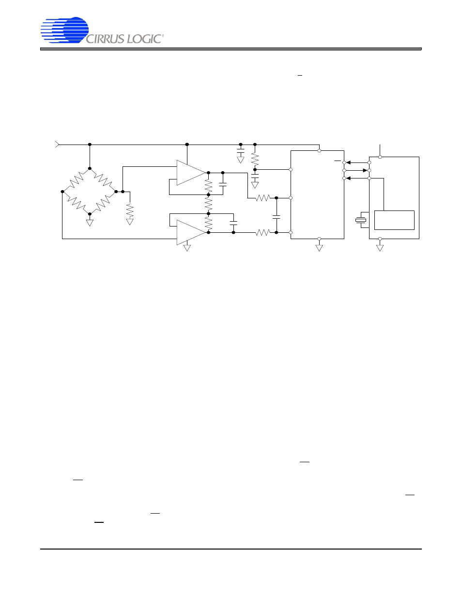
4. CS3002 AND CS5512 COMBINATION CIRCUIT WITH BRIDGE OFFSET
With two op amps the noise due to the amplifiers will increase by a factor of
√
2, (1.41). But this amplifier configura-
tion has the advantage that each input has high impedance and it is much easier to add components to perform
RFI filtering. This will be discussed in a later paragraph.
Figure 7.
In this third circuit, the CS5510/CS5512 is used in combination with the CS3002 dual op amp. Note that there is the
CS3012 dual with half the power consumption but twice the noise of the CS3002 if lower power consumption is a
requirement. The circuit can be configured in either of two ways, dependent upon the choice of resistors. In one
configuration, the output of the bridge is amplified and input into the ADC without any offset being added. In this
case, only the positive input span of the ADC is used. In the second configuration, a resistor (the 86.6 k
Ω) causes
the bridge to output a negative offset when no force is applied. This causes the signal into the ADC to be offset into
the negative portion of the input span of the ADC. When the offset is added, the gain of the amplifier is increased to
allow a much larger portion of the ADC span to be utilized.
Let's first examine the circuit without offset. In this case the gain of the amplifier is 715. The full-scale signal from
the load cell under full load is 5 mV. The amplifier would then provide a full-scale signal into the ADC of 3.57 volts.
This value has been chosen because the full scale of the ADC is nominally 80% of 5 V into the VREF pin but worst
case can be as low as 72% (per the data sheet) so the full scale could be as low as 5 V times 0.72, or 3.6 V. In this
configuration, the system would use only 3.57 volts of the nominal 8-volt span (full differential) of the converter. Note
that the span could be as low as 7.2 V or as high as 8.8 V depending upon the gain error of the ADC. But if a nominal
value is used, the circuit will use only 3.57 / 8 or 44.6% of the output codes of the converter. With the CS5512, this
would be about 467,900 codes.
In the configuration where an offset is added to the bridge and the amplifier gain is doubled, the useful code range
is doubled to about 936,000 codes.
What about noise performance? Each op amp in the CS3002 exhibits 6 nV /
√
Hz up to 2 kHz bandwidth. In the dif-
ferential-in-differential-out, two-amplifier configuration shown, the noise will increase by the square root of 2 to about
8.5 nV /
√
Hz.
In the previous circuit example it was indicated that the spot noise of the ADC would be about 939 nV /
√
Hz if
clocked at 200 kHz. With an amplifier gain of 715, the input-referred noise from the ADC to the input of the amplifiers
would be 939 / 715 = 1.31 nV /
√
Hz. Adding this in rms fashion to the 8.5 nV rms noise of the amplifiers will yield
about 8.6 nV /
√
Hz rms.
200
Ω
200
Ω
0 . 047
μF
V RE F
AIN+
AIN-
V -
V +
CS
S DO
SCLK
CS 5510/12
μC
+ 5 V
Counter / Timer
100
Ω
0. 1
μ F
+5 V
1 mV/V
-
+
350
Ω
0. 1
μ F
140 k
Ω
0. 22
μ F
CS 3002
( 86. 6 k
Ω)
-
+
-
+
140 k
Ω
0. 22
μ F
X 715
( X 1419)
R1
R2
R2
C2
C1
R 3
392
Ω
( 196
Ω )