Cirrus Logic AN330 REV2 User Manual
Page 6
6
AN330REV2
AN330
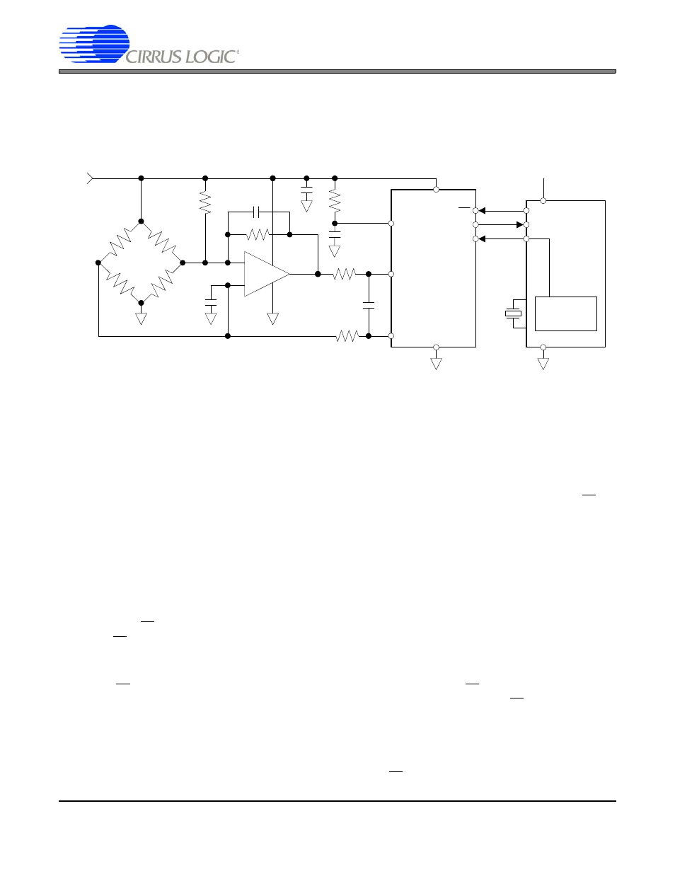
3. CS3001 AND CS5512 COMBINATION CIRCUIT WITH BRIDGE OFFSET
The second circuit is similar to the first. It uses a single CS3001 amplifier with a load cell to drive the CS5512 ADC.
The CS5512 device runs from an external continuous clock which is derived from the microcontroller to the SCLK
pin of the CS5512.
Figure 6.
The circuit shows the CS3001 set with a gain of 817X (the gain is 143 k / 175 ohm; the 175 is set by the parallel
combination of the two 350 ohm resistors inside the bridge). Note that few op amps can support a gain of 817x
(58 dB) and guarantee 16-bit or better linearity; the CS3001 will exhibit a 20-bit linearity. In this circuit the 88.7 k
resistor is added to offset the bridge to allow the input of the ADC to be negative with no weight on the load cell.
This allows more of the input span of the A/D converter to be used. The input of the ADC is ±4 V, fully differential.
Adding offset allows use of the negative range of the ADC. This provides more codes out of the converter for the
bridge signal.
The bridge has a sensitivity of 1 mV / V so it outputs 5 mV at full scale. The noise of the amplifier is 6 nV /
√
Hz.
The CS5512 can be driven from any clock rate from 10 kHz to 200 kHz. There are 612 clock cycles per conversion
so this means the CS5512 could output conversions at rates from 16.3 Sps to 326.7 Sps by changing its clock. The
noise in the converter is dominated by quantization noise and will be spread from DC to one half the output word
rate. This was illustrated with the plot of the CS5513 noise in Figure 3. The CS5512 and CS5513 use the same
modulator-filter design with the only difference being the clock source used to drive the chip. This means that with
the CS5512, the converter can achieve a lower spot noise if the output word rate is maximized. Running the con-
verter with a 200 kHz clock yields an output word rate of 326.7 Sps or an Fs / 2 bandwidth of 326.7 / 2 = 163.3 Hz.
Under this condition the spot noise (with VREF = 5 V) would be 12
μV rms divided by the square root of 163.3 or
about 939 nV /
√
Hz. If this value is divided by 817 and refered to the input of the CS3001 amplifier the result is
1.15 nV /
√
Hz. This is significantly below the spot noise of the op amp. Therefore, the op amp will be the dominant
source of the input-referred noise.
If the clock for the CS5512 was reduced to 32.768 KHz then the spot noise of the ADC would be about
2320 nV /
√
Hz. Referred to the input of the amplifier, this would become 2.84 nV /
√
Hz. This would increase the
input-referred noise of the system below the analog filter noise bandwidth to about 7.0 nV /
√
Hz.
To achieve maximum signal-to-noise performance, the bandwidth of the system should be limited. The 0.22
μF
capacitor across the 143 k
Ω resistor will limit the amplifier bandwidth to a single pole at 5 Hz. Additional filtering
can be achieved by averaging the output codes of the converter. If the converter outputs words at 326.7 Sps and
32 conversion words are averaged, this will result in an effective word rate of about 10 Sps and a noise bandwidth
of about 5 Hz. The signal will be 5 mV and the noise will be 7 nV /
√
Hz times the square root of 5, or
+5 V
1 mV/V
-
+
350
Ω
200
Ω
200
Ω
0.047
μF
0.1
μF
VREF
AIN+
AIN1
V-
V+
CS
SDO
SCLK
CS5510/12
μC
+5 V
Counter/Timer
-
+
0.22
μF
0.22
μF
CS3001
100
Ω
0.1
μF
143 k
Ω
88.7 k
Ω
Gain = 817