1 maximum peak current, 2 output bstout sense & input iac sense, 3 boost auxiliary winding – Cirrus Logic CS1613A User Manual
Page 10: 4 boost overvoltage protection
CS1610A/11A
CS1612A/13A
10
DS976F1
5.4.1
Maximum Peak Current
The maximum boost inductor peak current is set using
external resistor R
IPK
on pin IPK, which is sampled
periodically by an ADC. Maximum power output is proportional
to peak current code I
PK(code)
. See Equation 1:
where,
= a correction term of 0.55
V
rms(typ)
= nominal operating input RMS voltage
I
PK(BST)
= peak current code I
PK(code)
4.1mA
Resistor R
IPK
is calculated using peak current code I
PK(code)
.
5.4.2
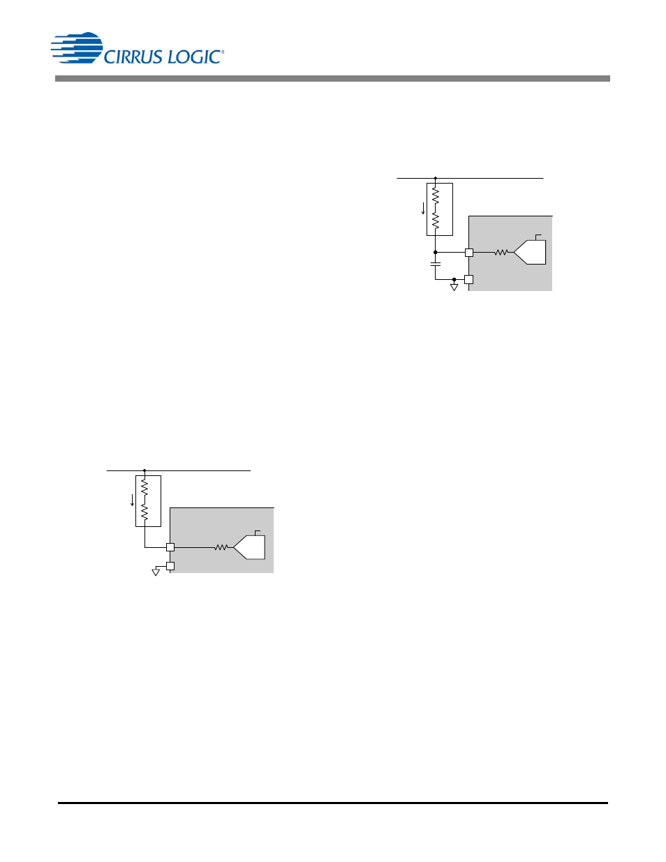
Output BSTOUT Sense & Input IAC
Sense
A current proportional to boost output voltage V
BST
is supplied
to the IC on pin BSTOUT and is used as a feedback control
signal (see Figure 12). The ADC is used to measure the
magnitude of current I
BSTOUT
through resistor R
BST
. The
magnitude of current I
BSTOUT
is then compared to an internal
reference current I
ref
of 133
A.
Resistor R
BST
sets the feedback current at the nominal boost
output voltage. For the CS1611A/13A, resistor R
BST
is
calculated as shown in Equation 3:
where,
V
BST
= nominal boost output voltage
I
ref
= internal reference current
For 120VAC line voltage applications (CS1610A/12A), nominal
boost output voltage V
BST
is 200V, and resistor R
BST
is 1.5M
.
By using digital loop compensation, the voltage feedback
signal does not require an external compensation network.
A current proportional to the AC input voltage is supplied to the
IC on pin IAC and is used by the boost control algorithm (see
Figure 13).
Resistor R
IAC
sets current I
AC
and is defined in Equation 4:
For optimal performance, capacitor C
IAC
should be connected
from pin IAC to ground in 230V circuits using the CS1611A or
CS1613A. Resistors R
IAC
and R
BST
should use 1% or better
resistors for best V
BST
voltage accuracy.
5.4.3
Boost Auxiliary Winding
The boost auxiliary winding is used for zero-current detection
(ZCD). The voltage on the auxiliary winding is sensed through
the BSTAUX pin of the IC. It is also used to deliver current
during steady-state operation, as mentioned in section 5.2
Startup Circuit
5.4.4
Boost Overvoltage Protection
The CS1610A/11A/12A/13A supports boost overvoltage
protection (BOP) to protect the bulk capacitor C8 (see
Figure 15). If the boost output voltage exceeds the
overvoltage protection thresholds of 249V for a 120V system,
or 448V for a 230V system, a BOP fault signal is generated.
The control logic continuously averages this BOP fault signal,
and if at any point in time the average exceeds a set event
threshold, the boost stage is disabled. The BOP fault
averaging algorithm sets the event threshold such that the
boost output voltage is never allowed to stay above the BOP
threshold for more than 1.6ms.
During a boost overvoltage protection event, the second stage
is kept enabled, and its dim input is railed to full scale. This
allows the second stage to dissipate the stored energy on bulk
capacitor C8 quickly, bringing down the boost output voltage
to a safe value. A visible flash on the LED might appear,
indicating that an overvoltage event has occurred. When the
boost output voltage drops to 195V for a 120V application or
368V for a 230V application, the boost stage is enabled, and
the system returns to normal operation.
P
IN max
I
PK BST
V
rms typ
2
-------------------------------------------------------------
=
[Eq.1]
R
IPK
4M
I
PK code
-----------------------
=
[Eq.2]
V
B S T
CS1610 A/ 11A/ 12A/13A
15k
ADC
R8
R
B S T
I
B S TOUT
R9
I
ref
16
BSTOUT
12
Figure 12. BSTOUT Input Pin Model
R
BST
V
BST
I
ref
--------------
400V
133
A
------------------
3M
=
=
[Eq.3]
R3
R
IA C
I
A C
I
A C
V
rect
15k
ADC
R4
2
I
ref
12
CS1610 A/11A/12A/13A
C
IA C
Figure 13. IAC Input Pin Model
R
IAC
R
BST
=
[Eq.4]