7 valley switching, Cs1501, Zcd_below _zero – Cirrus Logic CS1501 User Manual
Page 11
CS1501
DS927F4
11
Resistor R
IFB
sets the feedback current and is calculated as
follows:
By using digital loop compensation, the voltage feedback
signal does not require an external compensation network.
A current proportional to the AC input voltage is supplied to the
IC on pin IAC and is used by the PFC control algorithm.
Figure 17. IAC Input Pin Model
Resistor R
IAC
sets the I
AC
current and is derived as follows:
For optimal performance, resistors R
IAC
and R
IFB
should use
1% tolerance or better resistors for best V
link
voltage accuracy.
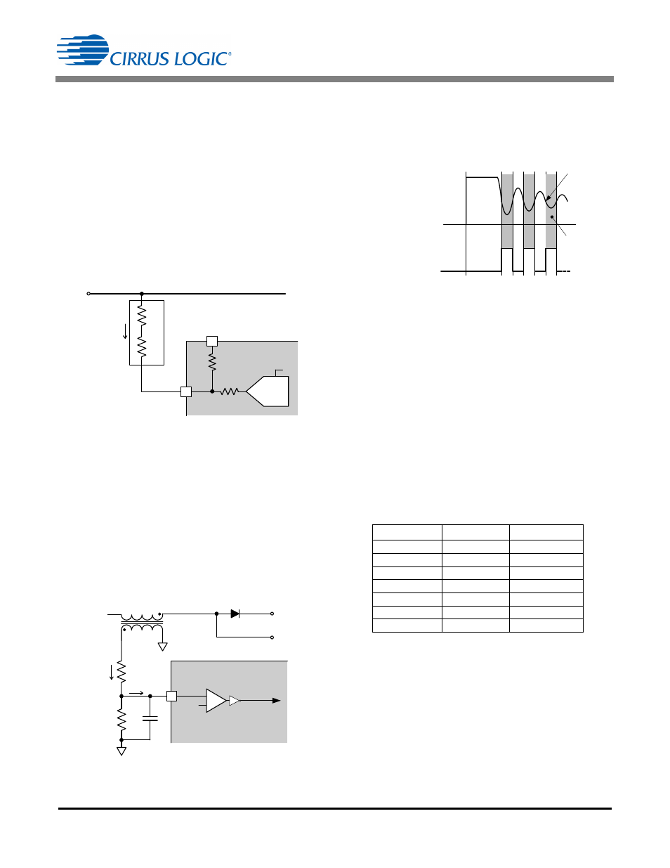
5.7 Valley Switching
The zero-current detection (ZCD) pin is monitored for
demagnetization in the auxiliary winding of the boost inductor
(L
B
). The ZCD circuit is designed to detect the V
Aux
valley/zero crossings by sensing the voltage transformed onto
the auxiliary winding of L
B
.
Figure 18. ZCD Input Pin Model
The objective of zero-voltage switching is to initiate each
MOSFET switching cycle when its drain-source voltage is at
the lowest possible voltage potential, thus reducing switching
losses. The CS1501 uses an auxiliary winding on the PFC
boost inductor to implement zero-voltage switching.
Figure 19. Zero-voltage Switch
During each switching cycle, when the boost diode current
reaches zero, the boost MOSFET drain-source voltage begins
oscillating at the resonant frequency of the boost inductor and
MOSFET parasitic output capacitance. The ZCD_below_zero
signal transitions from high to low just prior to a local minimum
of the MOSFET drain-source voltage oscillation. The
zero-crossing detect circuit ensures that a ZCD_below_zero
pulse will only be generated when the comparator output is
continuously high for a nominal time period (t
ZCB
) of 200ns.
Therefore, any negative edges on the comparator's output
due to spurious glitches will not cause a pulse to be
generated. Due to the CS1501’s variable-frequency control,
the MOSFET switching cycle will not always be initiated at the
first resonant valley.
The external circuitry should be designed so that the current
(I
ZCD
) at the ZCD pin is approximately
1.0 mA. The table
below depicts approximate values for R3 and R4 for a range
of boost-to-auxiliary inductor turns ratio, N.
Table 1. Aux Inductor Turns Ratio vs. R3 and R4
Resistors R3 and R4 were calculated using V
link
= 400V and
C
p
= 10pF.
Equation 6 is used to calculate the cut-off frequency defined
by the RC circuit at the ZCD pin.
where:
f
c
The cut-off frequency, f
c
, needs to be 10x the ringing
frequency
C
p
Capacitance at the ZCD pin
R
IFB
V
link
V
DD
–
I
ref
-----------------------------
400V V
DD
–
129
A
-------------------------------
=
=
[Eq.4]
R1
R
IAC
I
AC
IA C
V DD
15k
8
V
rect
CS1501
24k
ADC
R2
3
I
ref
R
IAC
R
IFB
=
[Eq.5]
R3
I
Aux
V
link
ZCD
L
B
R4
CS1501
ZCD_below_zero
D2
FE T Drain
N:1
+
V
Aux
-
Demag
Comparator
+
-
V
th( Z CD)
5
I
Z CD
C
p
N
~R3
~R4
9
46k
1.75k
10
42k
1.75k
11
37.5k
1.75k
12
35.5k
1.75k
13
32k
1.75k
14
29.5k
1.75k
15
27.5k
1.75k
ZCD
Zero Crossing
Detection
GD ‘ON’
ZCD_below _zero
f
c
1 2
R3 R4
C
p
=
[Eq.6]