3 burst mode, 4 output power and pfc boost inductor, 5 pfc output capacitor – Cirrus Logic CS1501 User Manual
Page 10: 6 output ifb sense and input iac sense, Cs1501
CS1501
10
DS927F4
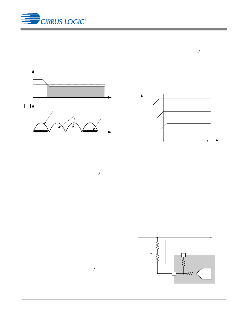
5.3 Burst Mode
Burst mode is used to improve system efficiency when the
system output power (P
o
) is <5% of nominal. Burst mode is
implemented by intermittently disabling the PFC over a full
half-line period under light-load conditions, as shown in
Figure 14.
Figure 14. Burst Mode
5.4 Output Power and PFC Boost Inductor
In normal operating mode, the nominal output power is
estimated by the following equation:
where:
P
o
rated output power of the system
efficiency of the boost converter (estimated as 100%
by the PFC algorithm)
V
in(min)
minimum RMS line voltage is 90V, measured after
the rectifier and EMI filter
V
link
nominal PFC output voltage (must be 400V)
f
max
maximum switching frequency is 70kHz
L
B
boost inductor specified by rated power requirement
<1
margin factor to guarantee rated output power (P
o
)
against boost inductor tolerances.
Equation 1 is provided for explanation purposes only. Using
substituted required design values for V
link
and f
max
gives the
following equation:
Changing the value for the V
link
voltage is not recommended.
Solving Equation 2 for the PFC boost inductor, L
B
, gives the
following equation:
If a value of the boost inductor other than that obtained from B , the link voltage V link will drop below 400V and fall out of regulation. Figure 15. Relative Effects of Varying Boost Inductance 5.5 PFC Output Capacitor The value of the PFC output capacitor needs to be selected F/watt to 2.0F/watt with a V link voltage of 400V. 5.6 Output IFB Sense and Input IAC Sense A current proportional to the PFC output voltage, V link , is supplied to the IC on pin IFB and is used as a feedback control IFB current through resistor R IFB . The magnitude of the I IFB current is then compared to an internal reference current (I ref ) of 129 A. Figure 16. IFB Input Pin Model V in [V] t [ms] FET V gs Burst Mode Active V in P o [W] t [ms] PFC Disable Burst Threshold P o V in min 2 V link V in min 2 – 2 f max L B V link --------------------------------------------------------- = [Eq.1] P o 90V 2 400V 90V 2 – 2 70kHz L B 400V ------------------------------------------------------------- = [Eq.2] L B 90V 2 400V 90V 2 – 2 70kHz P o 400V ------------------------------------------------------------- = [Eq.3] V AC(rms) 90 265 P o( m ax ) L > L B L = L B L < L B IFB V DD 15k 8 V link CS1501 24k ADC R5 R IFB I FB R6 1 I ref
Equation 3 above is used, the total output power capability
and the minimum input voltage threshold will differ according
to Equation 2. Note that if the input voltage drops below
90Vrms and the inductance value is
based upon voltage ripple and hold-up requirements. To
ensure system stability with the digital controller, the
recommended value of the capacitor is within the range of
0.5
signal. This current is compared against an internal
fixed-value reference current.
The ADC is used to measure the magnitude of the I