Bios setup, 1 chip configuration – Asus A7M266-D User Manual
Page 57
ASUS A7M266-D User’s Manual
57
4. BIOS SETUP
4. BIOS SETUP
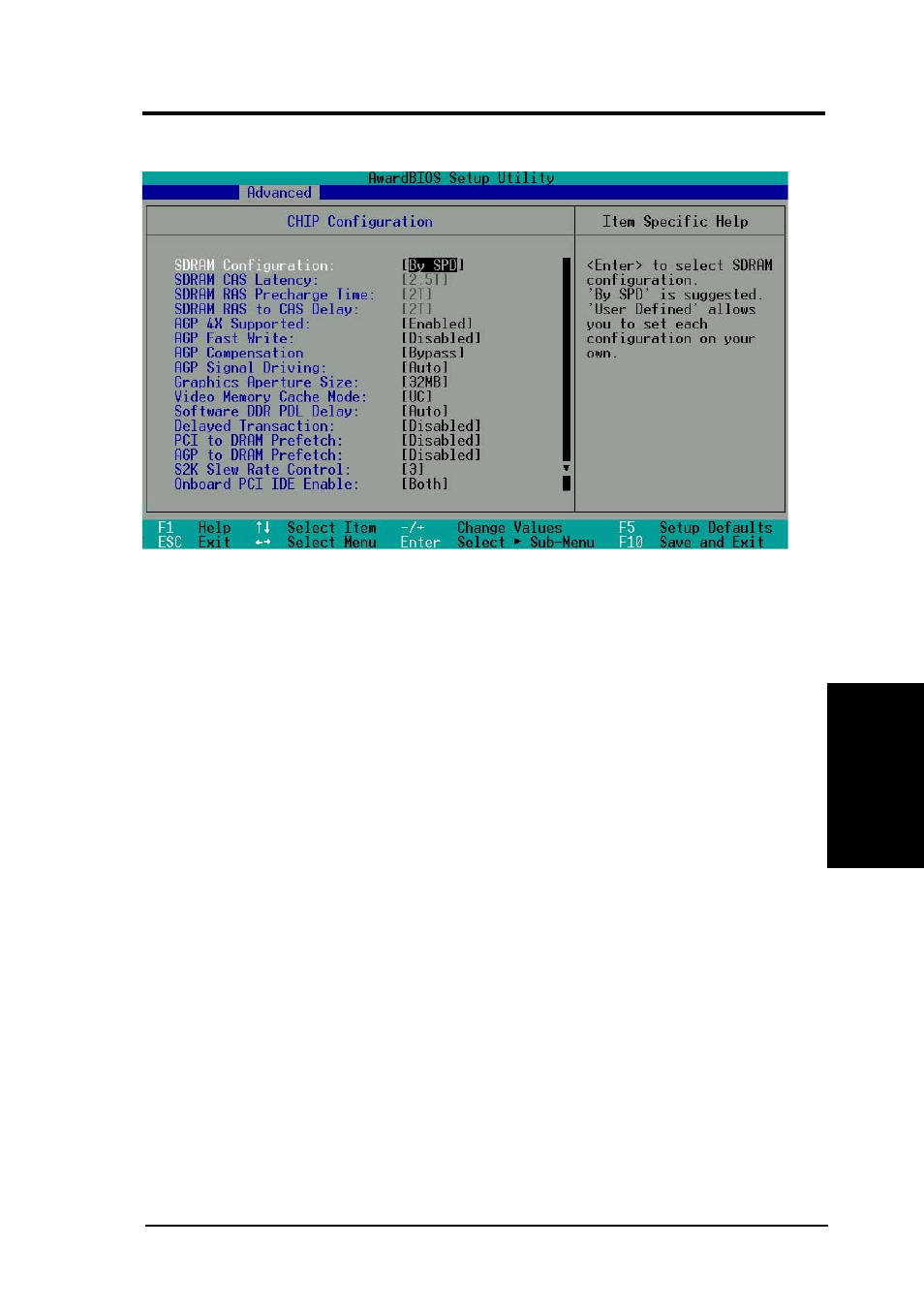
SDRAM Configuration [By SPD]
This sets the optimal timings for SDRAM related fields, depending on the
memory modules that you are using. Default setting is [By SPD], which
configures the subsequent 3 items by reading the contents in the SPD (Se-
rial Presence Detect) device. The EEPROM on the memory module stores
critical parameter information about the module, such as memory type, size,
speed, voltage interface, and module banks. Configuration options: [By
SPD][User Define]
SDRAM CAS Latency
This controls the latency between the SDRAM read command and the time
that the data actually becomes available. NOTE: This field will only be
adjustable when SDRAM Configuration is set to [User Define].
SDRAM RAS Precharge Time
This controls the idle clocks after issuing a precharge command to the
SDRAM. NOTE: This field will only be adjustable when SDRAM
Configuration is set to [User Define].
SDRAM RAS to CAS Delay
This controls the latency between the SDRAM active command and the
read/write command. NOTE: This field will only be adjustable when
SDRAM Configuration is set to [User Define].
AGP 4X Supported [Enabled]
This feature allows the CPU to write directly to the AGP card for up to 30%
performance gain over standard AGP 4X mode. Configuration options: [En-
abled] [Disabled]
4.4.1 Chip Configuration
Chip Configuration