2 cpld registers – AMD Geode LX CS5536 User Manual
Page 3
AMD Geode™ LX Processor DDR2 BIOS Porting Guide
3
46959A - March 2009
Application Note
3.2
CPLD Registers
The CPLD contains two registers that indicate how it
should assert the BA[1:0], A[12:0] signals and switch
enable signals.
• If accessing the registers via I2C, the register addresses
are 80h and 81h.
• If accessing with I/O, the addresses are AC10h and
AC11h.
The two registers are defined in Table 3-1 and 3-2. Instruct-
ing the CPLD to set or clear a signal causes the behavior to
occur immediately on its outputs.
Prior to executing a LOAD MODE command, the BIOS sets
the CPLD registers to the desired pattern. The DRAM reg-
isters are programmed with the A[n] signals. The register
being initialized is determined by the pattern on BA[1:0]
(MR=00b, EMR(1)=01b, EMR(2)=10b and EMR(3)=11b).
Then the BIOS generates the LOAD MODE command by
setting, and then clearing, the PROG_DRAM bit in the
MC_CF07_DATA register. AMD also recommends setting
the MSR_BA field (same register) to the desired BA[1:0]
levels (same procedure as initializing DDR).
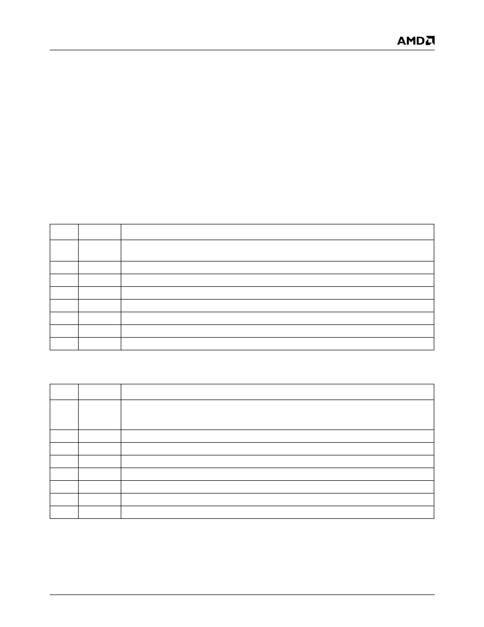
Table 3-1. REG_A Definition
Bit
Name
Description
7
A[7]
Address signal 7. If SW_EN# is high, setting this bit causes the CPLD to assert the A[7] signal.
This behavior is consistent for all the A[n] and BA[n] fields.
6
A[6]
Address signal 6
5
A[5]
Address signal 5
4
A[4]
Address signal 4
3
A[3]
Address signal 3
2
A[2]
Address signal 2
1
A[1]
Address signal 1
0
A[0]
Address signal 0
Table 3-2. REG_B Definition
Bit
Name
Description
7
SW_EN#
Switch enable. When high, the CPLD asserts all of its A[n] and BA[n] signals, according to the
current settings in the internal registers. When low, the CPLD closes the switches and tri-states
its A[n] and BA[n] signals.
6
BA[1]
Bank Address 1
5
BA[0]
Bank Address 0
4
A[12]
Address signal 12
3
A[11]
Address signal 11
2
A[10]
Address signal 10
1
A[9]
Address signal 9
0
A[8]
Address signal 8