0 solution, 1 hardware – AMD Geode LX CS5536 User Manual
Page 2
2
AMD Geode™ LX Processor DDR2 BIOS Porting Guide
46959A - March 2009
Application Note
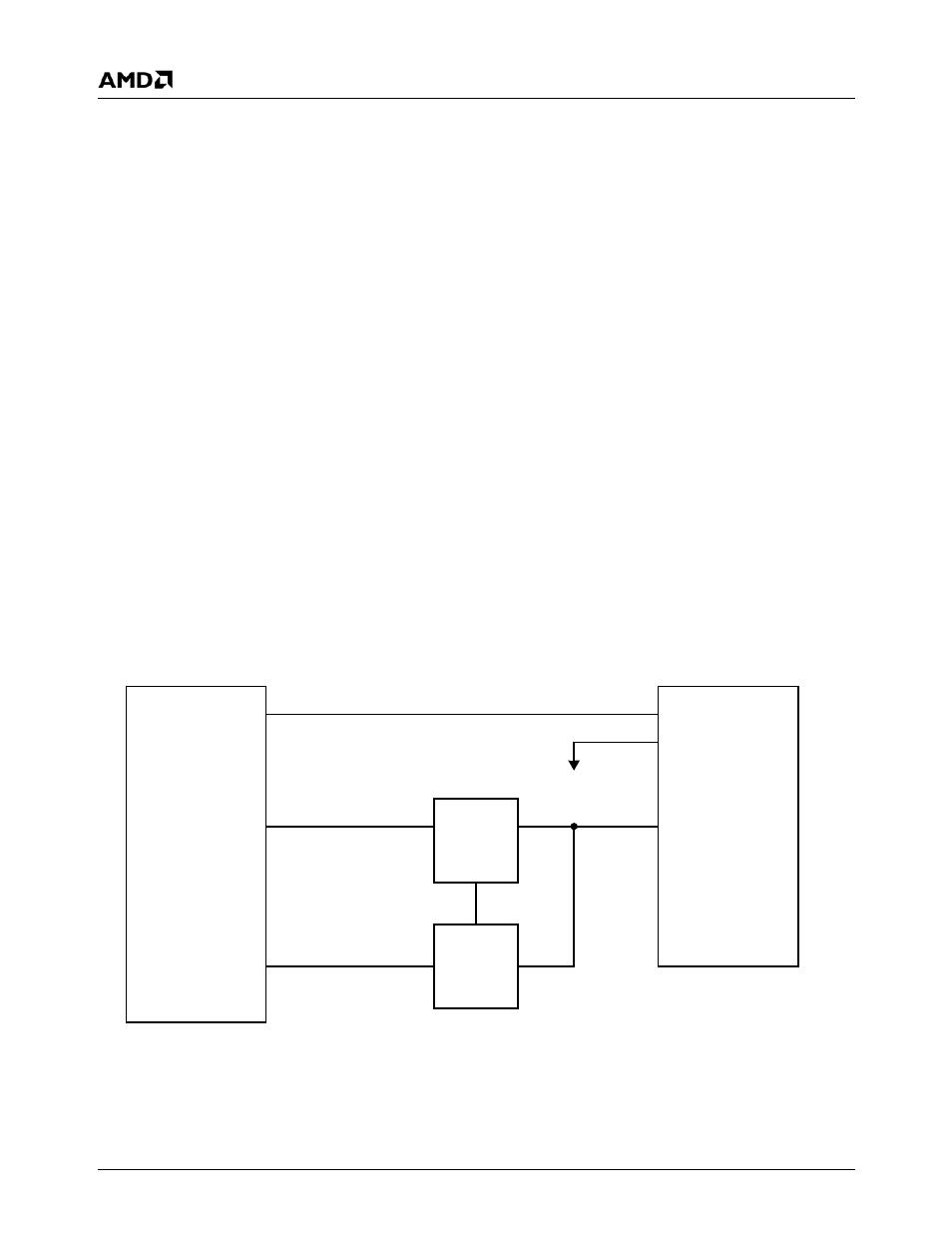
3.0 Solution
The method for initializing DDR2 memory on the processor
is to insert a CPLD and quick switches in the address and
BA signals. Figure 3-1 shows a block diagram of this
design. During initialization, the Enable signal opens
(default) the switches. BIOS tells the CPLD what pattern to
assert on the BA[n] and A[n] signals. Upon completion,
BIOS tells the CPLD to close the switches, giving control
over BA[n] and A[n] to the processor. Additional physical
and electrical details of the design are beyond the scope of
this document.
3.1
Hardware
This section explains the details of the initialization. First it’s
important to delineate two unique versions of this hardware
technology.
3.1.1
On-DIMM Design
This hardware form-factor has a DDR pin assignment (only
SO-DIMM as of this writing), but contains DDR2 SDRAM
modules, and the CPLD. This type of design will be attrac-
tive for customers wanting to upgrade existing systems.
The only board change required is a lower memory volt-
age.
Because the CPLD is contained on the DIMM assembly,
the only bus available for communication is I2C. The
CPLD’s I2C address is A0/A1 (i.e., the same as DIMM0).
The CPLD also contains the SPD information.
Also note that the CPLD uses CKE as its RESET# signal.
As a result, the list of BIOS changes may require moving
the assertion of CKE (e.g., if the SPD is accessed prior to
CKE).
3.1.2
On-board Design
This type of system will have the CPLD soldered onto the
motherboard, and will be able to use certain off-the-shelf
(OTS) DDR2 DIMMs. In this case, the CPLD does not con-
tain SPD information.
Because the communication is not limited to I2C, using I/O
to send data to the CPLD simplifies the CPLD design and
speeds up initialization.
The I/O addresses selected for the AMD Geode™ LX Pro-
cessor Refresh Reference Design Kit (RDK) board are
AC10h and AC11h. This requires a modification to the Vir-
tual PCI portion of the BIOS to identify the I/O range to an
operating system. As of this writing, the CPLD claims a
range of 8 bytes (i.e., AC10h-AC17h).
Figure 3-1. AMD Geode™ LX Processor DDR2 Block Diagram
AMD Geode™
LX Processor
/
CS5536
DDR2
SDRAM
A[13]
A[15:14],
BA[2]
Quick
Switches
A[12:0], BA[1:0]
CPLD
A[12:0],
BA[1:0]
Enable
I2C