Atmel AT89C5132 User Manual
Page 8
8
4173ES–USB–09/07
AT89C5132
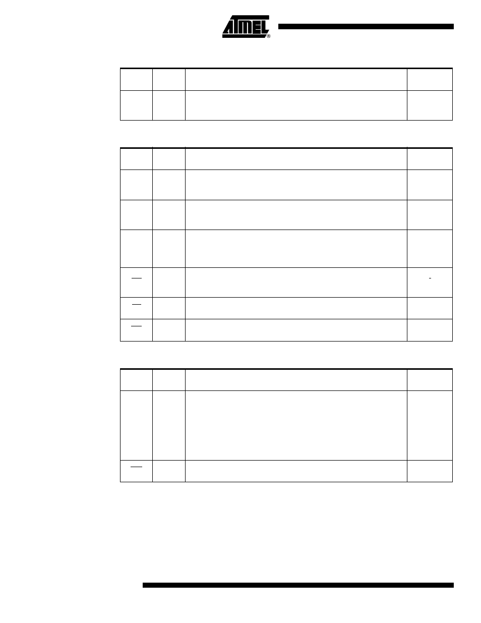
Table 11. Keypad Interface Signal Description
Table 12. External Access Signal Description
Table 13. System Signal Description
Signal
Name
Type
Description
Alternate
Function
KIN3:0
I
Keypad Input Lines
Holding one of these pins high or low for 24 oscillator periods triggers a
keypad interrupt.
P1.3:0
Signal
Name
Type
Description
Alternate
Function
A15:8
I/O
Address Lines
Upper address lines for the external bus.
Multiplexed higher address and data lines for the IDE interface.
P2.7:0
AD7:0
I/O
Address/Data Lines
Multiplexed lower address and data lines for the external memory or the IDE
interface.
P0.7:0
ALE
O
Address Latch Enable Output
ALE signals the start of an external bus cycle and indicates that valid address
information is available on lines A7:0. An external latch is used to demultiplex
the address from address/data bus.
-
ISP
I/O
ISP Enable Input
This signal must be held to GND through a pull-down resistor at the falling
reset to force execution of the internal bootloader.
-
RD
O
Read Signal
Read signal asserted during external data memory read operation.
P3.7
WR
O
Write Signal
Write signal asserted during external data memory write operation.
P3.6
Signal
Name
Type
Description
Alternate
Function
RST
I
Reset Input
Holding this pin high for 64 oscillator periods while the oscillator is running
resets the device. The Port pins are driven to their reset conditions when a
voltage lower than V
IL
is applied, whether or not the oscillator is running.
This pin has an internal pull-down resistor which allows the device to be reset
by connecting a capacitor between this pin and V
DD
.
Asserting RST when the chip is in Idle mode or Power-Down mode returns the
chip to normal operation.
-
TST
I
Test Input
Test mode entry signal. This pin must be set to V
DD
.
-