Atmel AT89C5132 User Manual
Page 6
6
4173ES–USB–09/07
AT89C5132
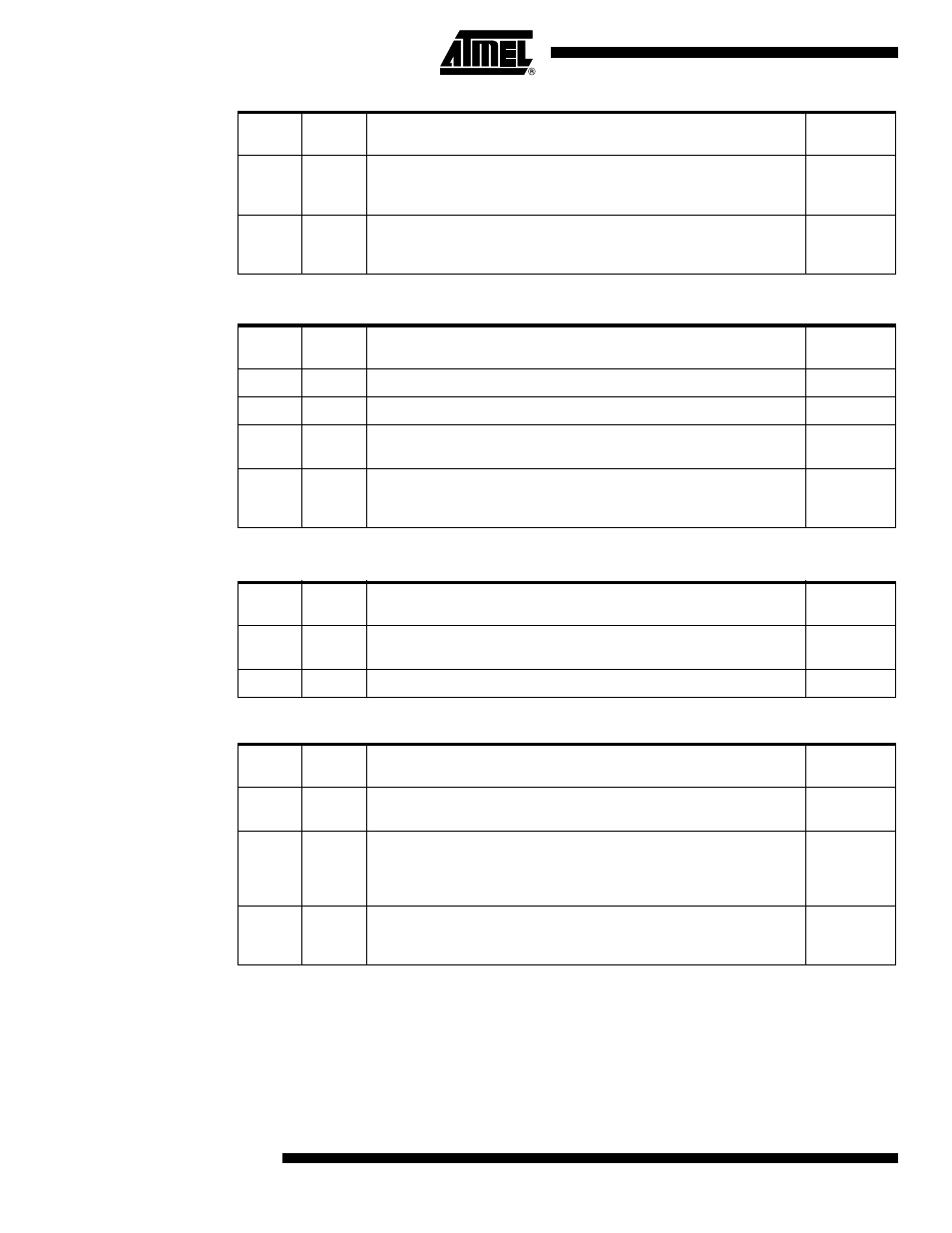
Table 4. Audio Interface Signal Description
Table 5. USB Controller Signal Description
Table 6. MutiMediaCard Interface Signal Description
T0
I
Timer 0 External Clock Input
When timer 0 operates as a counter, a falling edge on the T0 pin increments
the count.
P3.4
T1
I
Timer 1 External Clock Input
When timer 1 operates as a counter, a falling edge on the T1 pin increments
the count.
P3.5
Signal
Name
Type
Description
Alternate
Function
DCLK
O
DAC Data Bit Clock
-
DOUT
O
DAC Audio Data
-
DSEL
O
DAC Channel Select Signal
DSEL is the sample rate clock output.
-
SCLK
O
DAC System Clock
SCLK is the oversampling clock synchronized to the digital audio data (DOUT)
and the channel selection signal (DSEL).
-
Signal
Name
Type
Description
Alternate
Function
D+
I/O
USB Positive Data Upstream Port
This pin requires an external 1.5 K
Ω
pull-up to V
DD
for full speed operation.
-
D-
I/O
USB Negative Data Upstream Port
-
Signal
Name
Type
Description
Alternate
Function
MCLK
O
MMC Clock output
Data or command clock transfer.
-
MCMD
I/O
MMC Command line
Bidirectional command channel used for card initialization and data transfer
commands. To avoid any parasitic current consumption, unused MCMD input
must be polarized to V
DD
or V
SS
.
-
MDAT
I/O
MMC Data line
Bidirectional data channel. To avoid any parasitic current consumption, unused
MDAT input must be polarized to V
DD
or V
SS
.
-
Signal
Name
Type
Description
Alternate
Function