2 timings, 3 waveforms – Atmel AT89C5132 User Manual
Page 33
33
4173ES–USB–09/07
AT89C5132
6.3.9.2
Timings
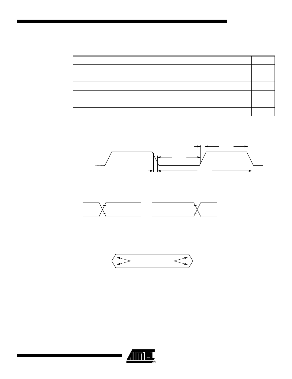
Table 22. External Clock AC Timings
V
DD
= 2.7 to 3.3V, T
A
= -40 to +85
°
C
6.3.9.3
Waveforms
Figure 6-23. External Clock Waveform
Figure 6-24. AC Testing Input/Output Waveforms
Notes:
1. During AC testing, all inputs are driven at
V
DD
-0.5V for a logic 1 and 0.45V for a logic 0.
2. Timing measurements are made on all outputs at V
IH
min for a logic 1 and V
IL
max for a logic 0.
Figure 6-25. Float Waveforms
Note:
For timing purposes, a port pin is no longer floating when a 100 mV change from load voltage occurs and begins to float when a
100 mV change from the loading V
OH
/V
OL
level occurs with I
OL
/I
OH
=
±
20 mA.
Symbol
Parameter
Min
Max
Unit
T
CLCL
Clock Period
50
ns
T
CHCX
High Time
10
ns
T
CLCX
Low Time
10
ns
T
CLCH
Rise Time
3
ns
T
CHCL
Fall Time
3
ns
T
CR
Cyclic Ratio in X2 Mode
40
60
%
0.45 V
T
CLCL
V
DD
- 0.5
V
IH1
V
IL
T
CHCX
T
CLCH
T
CHCL
T
CLCX
0.45 V
V
DD
- 0.5
0.7
V
DD
0.3
V
DD
V
IH
min
V
IL
max
INPUTS
OUTPUTS
V
LOAD
V
OH
- 0.1V
V
OL
+ 0.1V
V
LOAD
+ 0.1V
V
LOAD
- 0.1V
Timing Reference Points