1 signals – Atmel AT89C5132 User Manual
Page 4
4
4173ES–USB–09/07
AT89C5132
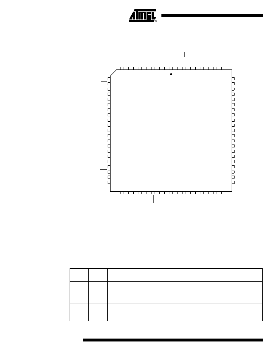
Figure 4-2.
AT89C5132 84-pin PLCC
(1)
Note:
1. For development board only.
4.1
Signals
All the AT89C5132 signals are detailed by functionality in Table 1 to Table 14.
Table 1. Ports Signal Description
PLCC84
P0.
3
/A
D
3
P0.
4
/A
D
4
P0.
5
/A
D
5
VS
S
VD
D
P0.
6
/A
D
6
P0.
7
/A
D
7
P2.
0
/A
8
P2.
1
/A
9
P
3
.3
/INT
1
P
3
.4/T
0
P
3
.5/T
1
P3.
6
/W
R
P
3
.2
/INT
0
65
64
63
62
61
60
59
58
55
56
57
12
13
14
15
16
17
22
20
19
33
34
35
36
37
4
3
2
1
84
83
82
81
80
79
78
NC
P2.3/A11
P2.4/A12
P2.6/A14
P2.5/A13
P2.7/A15
MCLK
MDAT
MCMD
P0.
2
/A
D
2
P0.
1
/A
D
1
P5.
0
PAVSS
VSS
X2
NC
X1
P3.
1
/T
X
D
18
21
23
24
25
38
39
40
41
42
69
68
67
66
70
5
6
7
8
9
P4.
3
/S
S
P4.
2
/S
C
K
P
4
.1
/M
OS
I
P
4
.0
/M
IS
O
VSS
VDD
RST
SCLK
DSEL
DCLK
DOUT
AI
N
1
AI
N
0
AR
E
F
N
AR
E
F
P
AV
S
S
AV
D
D
VS
S
VD
D
P
3
.7/R
D
P3
.0
/R
XD
P1.0/KIN0
P1.1/KIN1
P1.2/KIN2
P1.3/KIN3
P1.4
P1.5
P1.7/SDA
FILT
PAVDD
VDD
P1.6/SCL
26
43
TST
P5.
2
P0.
0
/A
D
0
77
P2.2/A10
54
ALE
ISP
NC
P5.
1
P4.
7
P4.
6
76
75
10
11
28
27
29
30
31
32
UVDD
UVSS
44
45
46
47
48
49
50
51
52
53
74
73
72
71
P4.4
P4.5
VDD
VSS
D-
D+
NC
P5.
3
Signal
Name
Type
Description
Alternate
Function
P0.7:0
I/O
Port 0
P0 is an 8-bit open-drain bidirectional I/O port. Port 0 pins that have 1s written
to them float and can be used as high impedance inputs. To avoid any parasitic
current consumption, floating P0 inputs must be polarized to V
DD
or V
SS
.
AD7:0
P1.7:0
I/O
Port 1
P1 is an 8-bit bidirectional I/O port with internal pull-ups.
KIN3:0
SCL
SDA