Pam8902h, Thermal information, Electrical characteristics – Diodes PAM8902H User Manual
Page 4
PAM8902H
Document number: DSxxxxx Rev. 1 - 0
4 of 12
December 2012
© Diodes Incorporated
PAM8902H
A Product Line of
Diodes Incorporated
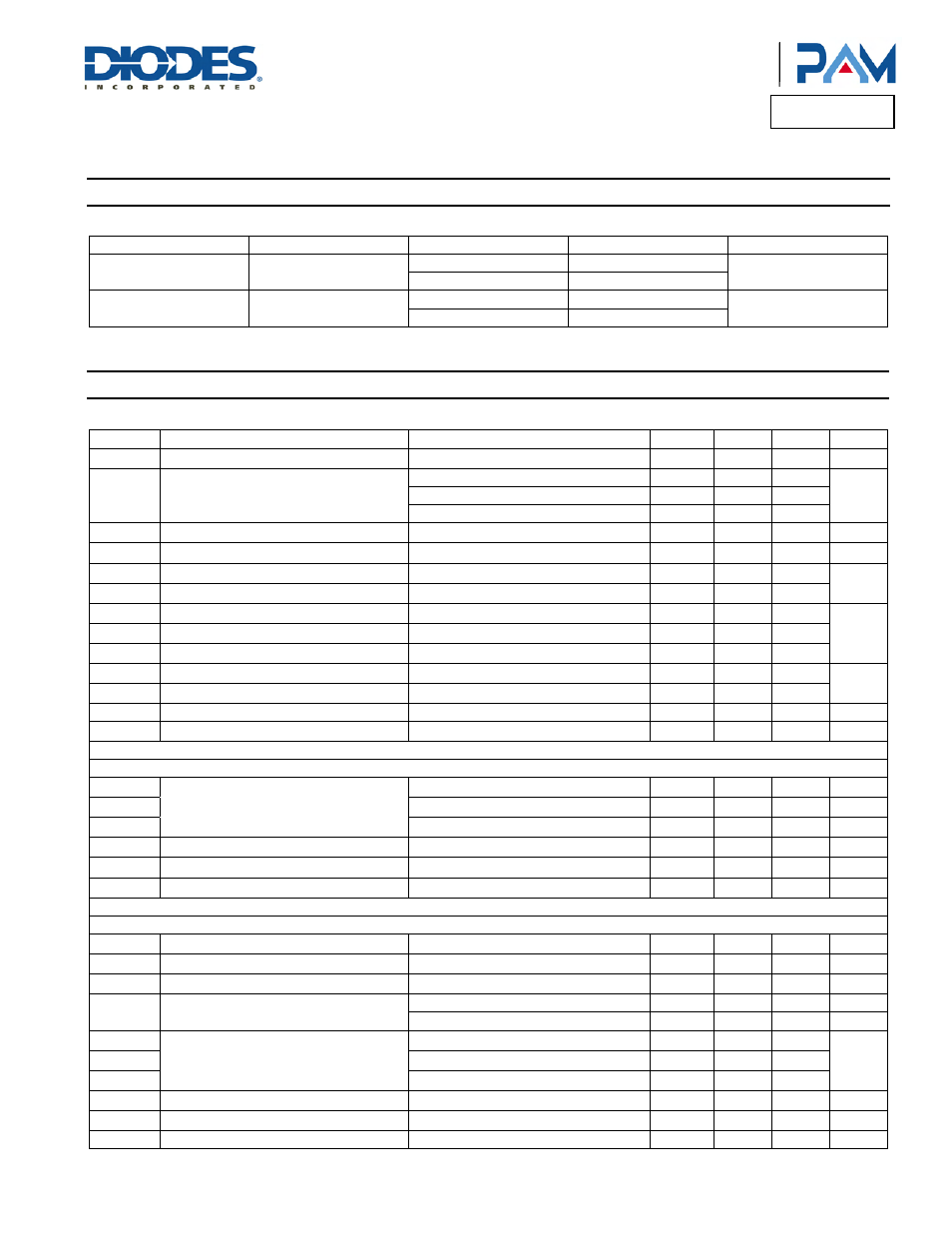
Thermal Information
Parameter Symbol Package Maximum
Unit
Thermal Resistance
(Junction to Ambient)
θ
JA
CSP 90
°C/W
QFN4x4-16 52
Thermal Resistance
(Junction to Case)
θ
JC
CSP 72
°C/W
QFN4x4-16 30
Electrical Characteristics
(@T
A
= +25°C, V
DD
= 3.6V, C
L
= 1µF, V
SET
Float, unless otherwise specified.)
Symbol Parameter
Conditions Min
Typ
Max
Unit
V
DD
Input Voltage
2.5
5.5
V
I
Q
Quiescent Current
EN > 1.2V, VSET = High
30
48
mA
EN > 1.2V, VSET = Floating
10
18
EN > 1.2V, VSET = GND
5
12
I
SD
Shutdown Current
EN = 0V
0.1
1.0
µA
T
WU
Wake-Up Time
EN From Low to High
40
mS
V
EH
Chip Enable
1.2
V
V
EL
Chip Disable
0.4
V
H
GSET/VSET High
V
DD
-0.5
V
DD
V
V
F
GSET/VSET Floating
1
V
DD
-1
V
L
GSET/VSET Low
0
0.5
UVLO
Under Voltage Lockout Threshold
V
DD
From High to Low
2.2
V
UVLO
H
Under Voltage Lockout Hysteresis
V
DD
From Low to High
0.2
OTP Thermal
Shutdown
Threshold
150
°C
OTP
H
Thermal Shutdown Lockout Hysteresis
30
°C
Boost Converter
V
O
1
Output Voltage
VSET = GND, No Load
7.2
8.0
8.8
V
V
O
2
VSET = NC, No Load
10.8
12.0
13.2
V
V
O
3
VSET = AVDD, No Load
16
17.5
19
V
C
L
Current Limit
Average Input Current
1.0
A
R
LS
Low Side MOSFET R
DS(ON)
I
O
= 50mA
0.5
Ω
f
OSCB
Boost Switching Frequency
1.1
1.5
1.9
MHz
Class-D
f
OSCD
Class-D Amplifier Switching Frequency
Input AC-GND
225
375
475
KHz
CMRR
Common Mode Reject Ratio
V
IN
= ±100mV, V
DD
= 3.6V
60 dB
V
OS
Output Offset Voltage
Output Offset Voltage
5
50
mV
R
P
R
DS(ON)
High Side
1.5
Ω
Low Side
0.6
Ω
A
V
1
Closed-Loop Voltage Gain
G
SET
= AVDD, V
O
= 1V
RMS
32.5
dB
A
V
2 G
SET
= AVDD, V
O
= 1V
RMS
26
A
V
3 G
SET
= AVDD, V
O
= 1V
RMS
21
PSRR
Power Supply Reject Ratio
200m V
PP
Supply Ripple @ 217Hz
70 dB
THD+N
Total Harmonice Distortion Plus Noise
V
O
= 5V
RMS
0.3 %
SNR
Signal to Noise Ratio
Input AC Ground, A-Weighting
90
dB