Pam8902, Application information – Diodes PAM8902 User Manual
Page 7
PAM8902
Document number: DSxxxxx Rev. 1 - 4
7 of 13
www.diodes.com
November 2012
© Diodes Incorporated
PAM8902
A Product Line of
Diodes Incorporated
Application Information
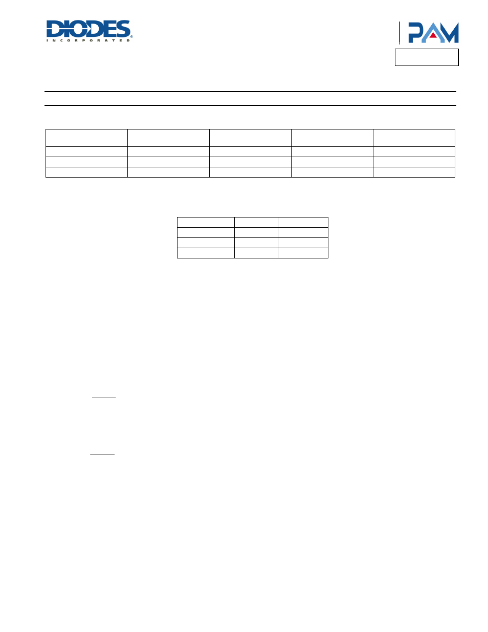
Select Boost Converter Output Voltage
Customer can use V
SET
pin to set boost converor output voltage between 8V, 12V and 17.5V. V
SET
pin configuration table as below:
V
SET
Pin Configuration
Min Max
PVCC
Voltage
Audio Amplifier
Maximum Output Voltage
Connect to AVDD
AVDD – 0.5
AVDD
17.5V
11 V
RMS
(V
PP
= 31.1V)
Floating
1V
AVDD – 1V
12V
8 V
RMS
(V
PP
= 22.6V)
Connect to GND
GND
0.5V
8V
5 V
RMS
(V
PP
= 14.1V)
Input Resistance (R
I
)
The input resistors (R
I
= R
IN
+ R
EX
) set the gain of the amplifier according to Equation 1 when anti-saturation is inactive.
G = 20 Log [12.8*R
F
/ (R
IN
+ R
EX
)] (dB)
G
SET
R
IN
R
FB
G
SET
= V
DD
77.4kΩ 122.6kΩ
G
SET
= Floating
100kΩ 100kΩ
G
SET
= GND
122.6kΩ 77.4kΩ
Where R
IN
is a 77.4KΩ internal resistor, R
EX
is the external input resistor, R
F
is a 122.6KΩ internal resistor. Resistor matching is very important
in fully differential amplifiers. The balance of the output on the reference voltage depends on matched ratios of the resistors. CMRR, PSRR, and
cancellation of the second harmonic distortion diminish if resistor mismatch occurs. Therefore, it is recommended to use 1% tolerance resistors
or better to keep the performance optimized. Matching is more important than overall tolerance. Resistor arrays with 1% matching can be used
with a tolerance greater than 1%. Place the input resistors very close to the PAM8902 to limit noise injection on the high-impedance nodes. For
optimal performance the gain should be set to lower. Lower gain allows the PAM8902 to operate at its best, and keeps a high voltage at the input
making the inputs less susceptible to noise. In addition to these features, higher value of R
I
minimizes pop noise.
Input Capacitors (C
I
)
In the typical application, an input capacitor, C
I
, is required to allow the amplifier to bias the input signal to the proper DC level for optimum
operation. In this case, Ci and the minimum input impedance R
I
form is a high-pass filter with the corner frequency determined in the follow
equation:
C
R
2
1
F
I
I
C
It is important to consider the value of C
I
as it directly affects the low frequency performance of the circuit.
For example, when R
I
is 150k and the specification calls for a flat bass response are down to 150Hz.
Equation is reconfigured as followed:
R
2
1
C
IFC
I
When input resistance variation is considered, the C
I
is 7nF, so one would likely choose a value of 10nF. A further consideration for this
capacitor is the leakage path from the input source through the input network (C
I
, R
I
+ R
F
) to the load. This leakage current creates a DC offset
voltage at the input to the amplifier that reduces useful headroom, especially in high gain applications. For this reason, a low-leakage tantalum or
ceramic capacitor is the best choice. When polarized capacitors are used, the positive side of the capacitor should face the amplifier input in
most applications as the DC level is held at V
DD
/2, which is likely higher than the source DC level. Please note that it is important to confirm the
capacitor polarity in the application.