Pam2863, Thermal information, Electrical characteristics – Diodes PAM2863 User Manual
Page 4
PAM2863
Document number: DSxxxxx Rev. 1 - 0
4 of 11
www.diodes.com
October 2012
© Diodes Incorporated
PAM2863
A Product Line of
Diodes Incorporated
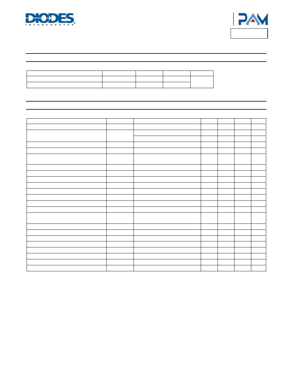
Thermal Information
Parameter Package
Symbol
Max
Unit
Thermal Resistance (Junction to Ambient)
SOP-8(EP)
θ
JA
90
°C/W
Thermal Resistance (Junction to Case)
SOP-8(EP)
θ
JC
11
Electrical Characteristics
(@T
A
= +25°C, V
IN
= 16V, unless otherwise specified.)
Parameter Symbol
Test
Conditions
Min
Typ
Max
Units
Inout Voltage
V
IN
4.5 40 V
Output Current
I
LED
R
S
= 0.1Ω
1 A
R
S
= 0.05Ω
2 A
Shutdown Current
I
SD
VSET Pin Grounded
20
40
µA
Quiescent Current without Switching
I
Q
VSET Pin Floating, V
IN
= 16V
0.6 mA
Mean Current Sense Threshold Voltage
V
SENSE
Measured on I
SENSE
Pin with
Respect to V
IN
95 100 105 mV
Sense Threshold Hysteresis
V
SENSE_HYS
±13
%
ISENSE Pin Input Current
I
SENSE
V
SENSE
= V
IN
-0.1
8
µA
VSET Range on VSET Pin
V
EN
For DC Dimming
0.3
2.5
V
DC Voltage on VSET Pin to Enable
V
EN(ON)
V
EN
Rising
0.25 V
DC Voltage on VSET Pin to Disable
V
EN(OFF)
V
EN
Falling
0.2 V
LX Switch on Resistance
R
LX
@I
LX
= 100mA
0.3 Ω
LX Switch Leakage Current
I
LX(LEAK)
5
µA
Soft-Start Time
T
SS
V
IN
= 16V, C
EN
= 1nF
1.5 Ms
Operating Frequency
F
LX
V
IN
= 16V, V
O
= 9.6V (3 LEDs),
L = 47µH, ΔI = 0.25A (I
LED
= 1A)
233 kHz
Recommended Minimum Switch ON Time
T
ON_REC
For 4% Accuracy
500 Ns
Recommended Maximum Switch Frequency
F
LX(MAX)
1.0
MHz
Max Duty Circle
98 %
Recommended Duty Cycle Range
D
LX
25 75
%
Internal Comparator Propagation Delay
T
PD
(Note 1)
45 Ns
Over Temperature Protection
T
OTP
150 °C
Temp Protection Hysteresis
T
OTP_HYS
40 °C
Current Limit
I
XL(MAX)
Peak Inductor Current
2.5 A
Note: 1.
V
SENSE
: LevelA: 95mV to 100mV; level B: 100mV to 105mV
Parameters are not tested at production, but guaranteed by design.