Pam3131, Pin description, Functional block diagram – Diodes PAM3131 User Manual
Page 2: Absolute maximum ratings
PAM3131
Document number: DSxxxxx Rev. 1 - 1
2 of 14
October 2012
© Diodes Incorporated
PAM3131
A Product Line of
Diodes Incorporated
Pin Description
Pin Name
Pin Number
Function
TO263-5L PSOP-8(EPD)
VIN
1 2
Input
EN
2 3
Enable
Pin
ADJ
4 6
Adjustable
Pin
VOUT
5 7
Output
GND
3
1, 4, 8
Ground
PWRGD —
5
Power
Good
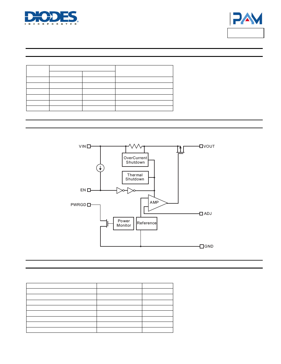
Functional Block Diagram
Absolute Maximum Ratings
(@T
A
= +25°C, unless otherwise specified.)
These are stress ratings only and functional operation is not implied. Exposure to absolute maximum ratings for prolonged time periods may
affect device reliability. All voltages are with respect to ground.
Parameter Rating
Unit
Input Voltage
4.0
V
Output Pin Voltage
-0.3 to V
IN
+0.3
V
Operation Temperature Range
-40 to +85
°C
Operation Junction Range
-40 to +125
°C
Maximum Output Current
P
D
/(V
IN
–V
O
)
—
Storage Temperature
-65 to +150
°C
Maximum Junction Temperature
150
°C
Soldering Temperature
300, (5sec)
°C