Pam2841, Application information, Ordering information – Diodes PAM2841 User Manual
Page 12
PAM2841
Document number: DSxxxxx Rev. 1 - 5
12 of 16
September 2013
© Diodes Incorporated
PAM2841
A Product Line of
Diodes Incorporated
Application Information
(cont.)
Layout Consideration
As for all switching power supplies, especially those in high frequency and high current ones, layout is an important design step. If layout is not
carefully done, the regulator could suffer from instability as well as noise problems.
(1) Use separate traces for power ground and signal ground. Power ground and signal ground are connected together to a quite ground (input
connector).
(2) To prevent radiation of high frequency resonance, proper layout of the high frequency switching path is essential. Minimize the length and
area of all traces connecting to the SW pin. The loop including the PWM switch, schottky diode and output capacitor, contains high current
rising and falling in nanosecond and thus it should be kept as short as possible.
(3) The input capacitor should be close to both the VIN pin and the GND pin in order to reduce the IC supply ripple.
(4) Keep the signal ground traces short and as close to the IC as possible. Small signal components should be placed as close as possible to the
IC, thus minimizing control signal noise interference.
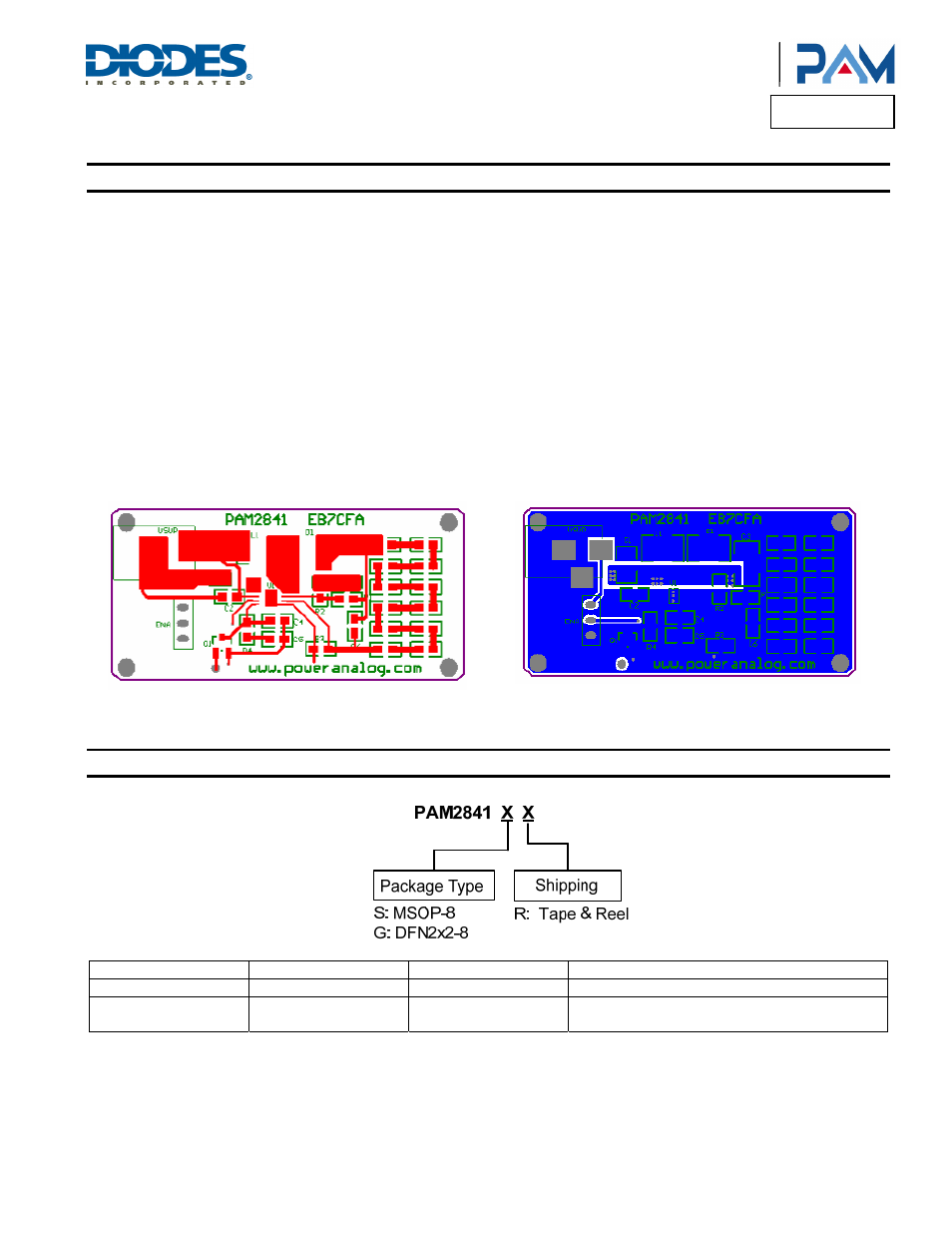
Layout Example
Top Layer
Bottom Layer
Ordering Information
Part Number
Part Marking
Package Type
Standard Package
PAM2841SR
P2841
MSOP-8
2500 Units/Tape & Reel
PAM2841GR
EMX
YW
DFN2x2-8
3000 Units/Tape & Reel