Pam2321, Typical applications circuit, Pin descriptions – Diodes PAM2321 User Manual
Page 2: Functional block diagram
PAM2321
Document number: DSxxxxx Rev. 2 - 1
2 of 11
January 2013
© Diodes Incorporated
PAM2321
A Product Line of
Diodes Incorporated
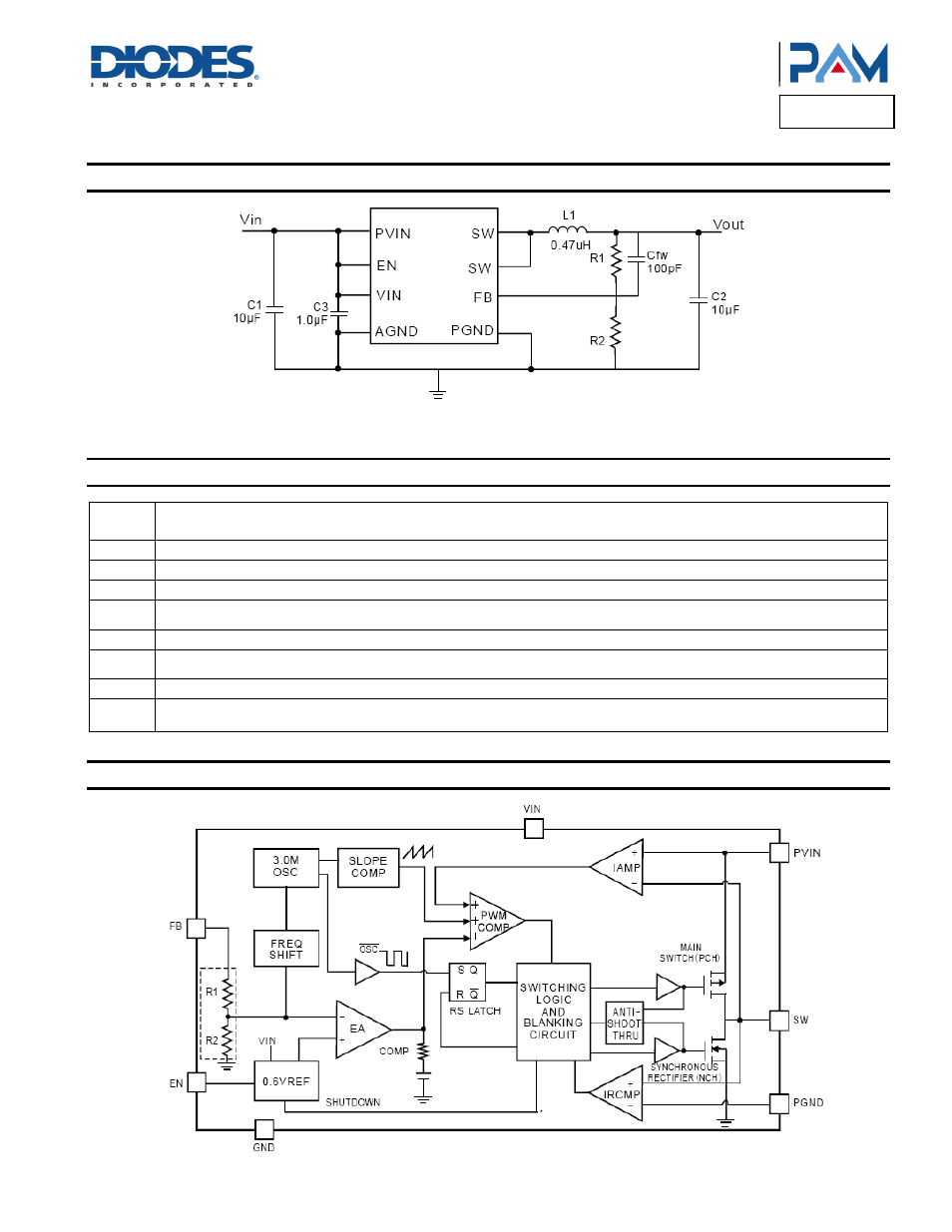
Typical Applications Circuit
(
)
2
R
/
1
R
1
*
6
.
0
V
OUT
+
=
Pin Descriptions
Pin
Name
Function
PGND
Main power ground return pin. Connect to the output and input capacitor return.
PVIN
Input power supply tied to the source of the high side P-Channel MOSFET.
VIN
Power supply; supplies power for the internal circuitry.
FB
Feedback input pin. This pin is connected directly to the converter output for the 1.2V fixed output version, or connected to an
external resistor divider for the adjustable output version.
AGND
Analog ground. This pin is internally connected to the analog ground of the control circuitry.
EN
Enable pin. A logic low disables the converter and it consumes less than 1μA of current. When connected high, it resumes normal
operation.
SW
Switching node. Connect the inductor to this pin. It is internally connected to the drain of both high and low side MOSFETs.
EP
Exposed pad of the package provides both electrical contact to the ground and good thermal
contact to the PCB. This pad must be soldered to the PCB for proper operation.
Functional Block Diagram