Pam2316, Typical applications circuit, Pin descriptions – Diodes PAM2316 User Manual
Page 2: Functional block diagram
PAM2316
Document number: DSxxxxx Rev. 1 - 1
2 of 11
www.diodes.com
November 2012
© Diodes Incorporated
PAM2316
A Product Line of
Diodes Incorporated
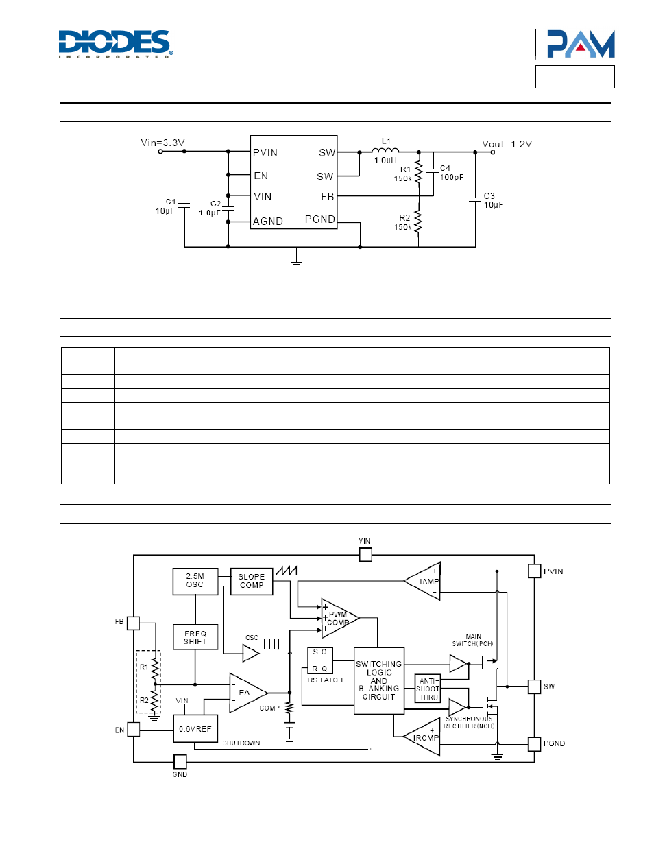
Typical Applications Circuit
V
OUT
= 0.6* (1+R1/R2)
Pin Descriptions
Pin
Number
Pin
Name
Function
1 PGND
Main power ground return pin. Connect to the output and input capacitor return.
2 PVIN
Input power supply tied to the source of the high side P-channel MOSFET.
3 VIN
Power supply; supplies power for the internal circuitry.
4 FB
Feedback input pin. Feedback voltage to internal error amplifier, the threshold voltage is 0.6V.
5 AGND
Analog ground. This pin is internally connected to the analog ground of the control circuitry.
6 EN
Enable pin. A logic low disables the converter and it consumes less than 1μA of current.When connected high, it
resumes normal operation.
7, 8
SW
Switching node. Connect the inductor to this pin. It is internally connected to the drain of both high and low side
MOSFETs.
Functional Block Diagram