Pam2308, Application information – Diodes PAM2308 User Manual
Page 12
PAM2308
Document number: DSxxxxx Rev. 1 - 1
12 of 15
January 2013
© Diodes Incorporated
PAM2308
A Product Line of
Diodes Incorporated
Application Information
(cont.)
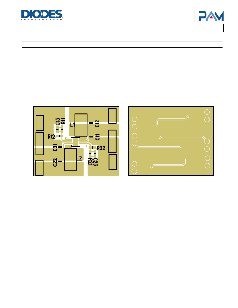
PCB Layout Check List
When laying out the printed circuit board, the following checklist should be used to ensure proper operation of the PAM2308. These items are
also illustrated graphically in Figure 1. Check the following in your layout:
1. The power traces, consisting of the GND trace, the SW trace and the V
IN
trace should be kept short, direct and wide.
2. Does the FB pin connect directly to the feedback resistors? The resistive divider R1/R2 must be connected between the (+) plate of C
OUT
and
ground.
3. Does the (+) plate of C
IN
connect to V
IN
as closely as possible? This capacitor provides the AC current to the internal power MOSFETs.
4. Keep the switching node, SW, away from the sensitive FB node.
5. Keep the (–) plates of C
IN
and C
OUT
as close as possible.
Top Bottom
Figure 1. PAM2308 Suggested Layout