Pam2307, Typical applications circuit, Pin descriptions – Diodes PAM2307 User Manual
Page 2: Functional block diagram
PAM2307
Document number: DSxxxxx Rev. 2 - 1
2 of 14
www.diodes.com
September 2012
© Diodes Incorporated
PAM2307
A Product Line of
Diodes Incorporated
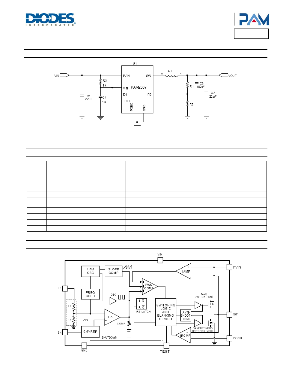
Typical Applications Circuit
V
2
R
1
R
1
6
.
0
O
⎟
⎟
⎠
⎞
⎜
⎜
⎝
⎛
+
×
=
Pin Descriptions
Pin
Name
Package Name
Function
QFN3x3-16L SOP-8(EP)
PGND
1, 2, 3
2
Main power ground pin.
FB 4
3
Feedback voltage to internal error amplifier, the threshold voltage is 0.6V.
GND 5
4
Signal ground for small signal components.
NC 6,
16
—
No connection.
EN 7
5
Enable control input. Force this pin voltage above 1.5V, enables the chip, and
below 0.3V shuts down the device.
TEST 8
6
Test Mode(no connect or to Ground).
VIN 9
7
Bias supply. Chip main power supply pin.
PVIN
10, 11, 12
8
Input supply for power stage. Must be closely decoupled to PGND.
SW
13, 14, 15
1
The drains of the internal main and synchronous power MOSFET.
Functional Block Diagram
- PDS3200 (5 pages)
- PDS340 (5 pages)
- PDS340Q (5 pages)
- PDS360 (5 pages)
- PDS360Q (5 pages)
- PDS4150 (4 pages)
- PDS3100Q (5 pages)
- PDS3100 (5 pages)
- PDS1240CTL (5 pages)
- PDS1045 (5 pages)
- PDS1040L (5 pages)
- PDS1040CTL (5 pages)
- PDS1040 (5 pages)
- PD3S230L (5 pages)
- PD3S230H (3 pages)
- PDS5100Q (5 pages)
- PDS835L (5 pages)
- PDS760 (5 pages)
- PDS560 (5 pages)
- PDS540 (5 pages)
- PDS5100H (5 pages)
- PDS5100 (5 pages)
- PDS4200H (6 pages)
- SBL3060CTP (4 pages)
- SBL30L30CT (3 pages)
- SBL3045CTP (4 pages)
- SBL3040CTP (4 pages)
- SBL2060CTP (4 pages)
- SBL2030CT - SBL2060CT (3 pages)
- SBL2045CTP (4 pages)
- SBL1060CTP (4 pages)
- SBL1040CTP (4 pages)
- SBG3030CT - SBG3045CT (5 pages)
- SB520 - SB560 (3 pages)
- SB370 - SB3100 (3 pages)
- SB320 - SB360 (3 pages)
- SBR10U100CT (5 pages)
- SBR10U150CT (5 pages)
- SBR10A45SP5 (5 pages)
- SBR1060CT (5 pages)
- SBR1045SP5 (5 pages)
- SBR1045SD1 (4 pages)
- SBR1045D1 (5 pages)
- SBR1045CTL (4 pages)
- SBR1040CT (5 pages)