Pin descriptions, Functional block diagram – Diodes PAM2423 User Manual
Page 2
PAM2421/PAM2422/PAM2423
Document number: DSxxxxx Rev. 1 - 1
2 of 10
www.diodes.com
November 2012
© Diodes Incorporated
PAM2421/ PAM2422/ PAM2423
A Product Line of
Diodes Incorporated
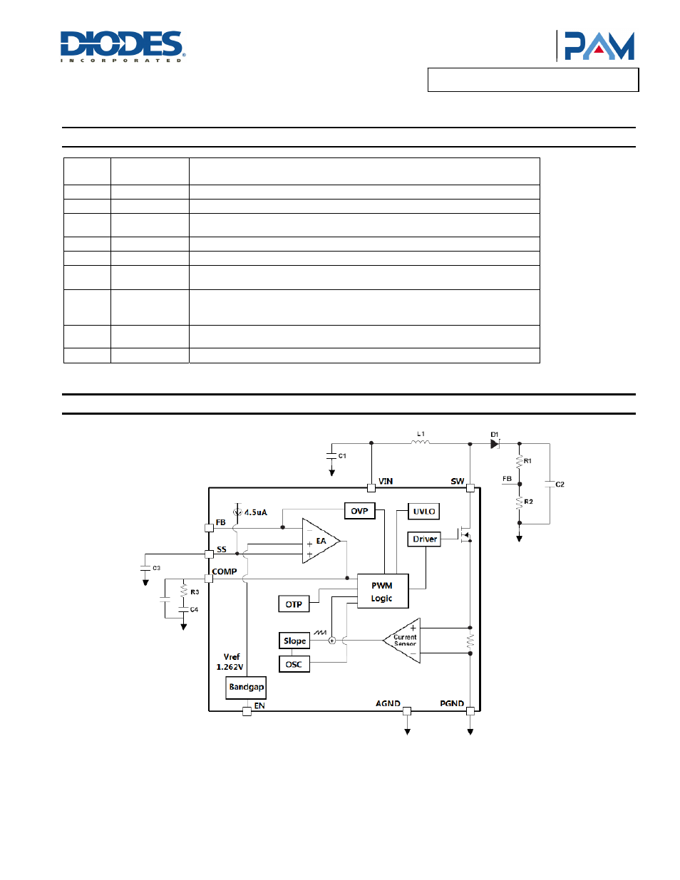
Pin Descriptions
Pin
Number
SOP-8(EP)
Pin Name
Function
1 PGND
Power Ground
2 IN
Supply Input
3 EN
Enable Control. Connect to a logic high level to enable the IC. Connect to a logic low
level to disable the IC. When unused, connect EN pin to IN (do not leave pin floating).
4 COMP
Error Amplifier Compensation Node
5 AGND
Analog Ground
6 FB
Feedback Input.Connect this pin a resistor divider from the output to set the output
voltage. FB is regulated to 1.262V.
7 SS
Soft Start Control Input. Connect a capacitor from this pin to Ground to set soft-start
timing duration. SS is discharged to ground in shutdown. SS may be left unconnected if
soft start is not desired.
8 SW
Switch Output. Connect this pin to the inductor and the schottky diode. To minimize
EMI, minimize the PCB trace path between this pin and the input bypass capacitor.
— Exposed
PAD
Connected to Ground
Functional Block Diagram