Maximum ratings, Electrical characteristics, Mmst6427 – Diodes MMST6427 User Manual
Page 2

MMST6427
Document number: DS30166 Rev. 11 - 2
2 of 5
August 2011
© Diodes Incorporated
MMST6427
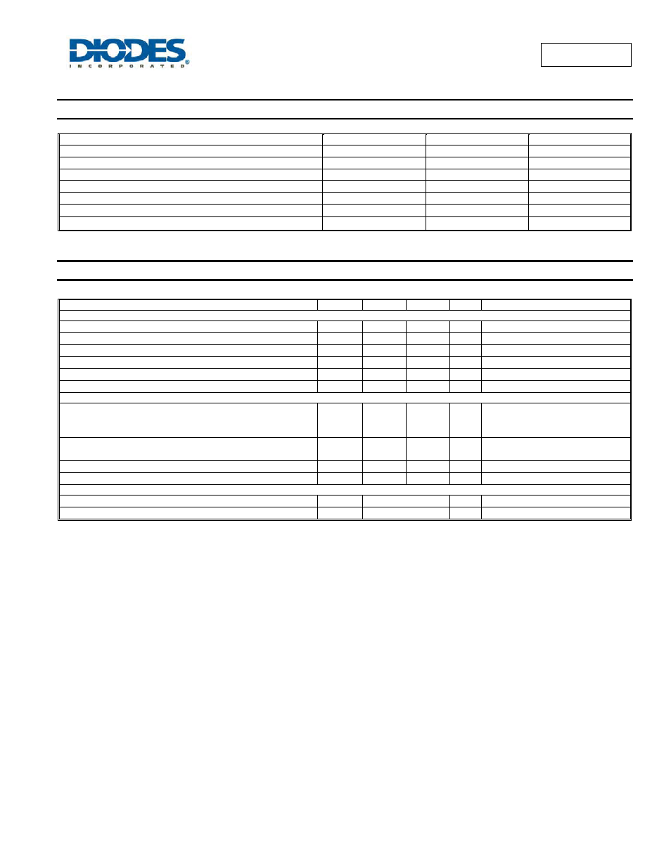
Maximum Ratings
@T
A
= 25°C unless otherwise specified
Characteristic
Symbol
Value
Unit
Collector-Base Voltage
V
CBO
40
V
Collector-Emitter Voltage
V
CEO
40
V
Emitter-Base Voltage
V
EBO
12
V
Collector Current - Continuous (Note 4)
I
C
500
mA
Power Dissipation (Note 4)
P
d
200
mW
Thermal Resistance, Junction to Ambient (Note 4)
R
θJA
625
°C/W
Operating and Storage Temperature Range
T
j
, T
STG
-55 to +150
°C
Electrical Characteristics
@T
A
= 25°C unless otherwise specified
Characteristic
Symbol
Min
Max
Unit
Test Condition
OFF CHARACTERISTICS (Note 5)
Collector-Base Breakdown Voltage
BV
CBO
40
⎯
V
I
C
= 100
μA, I
E
= 0
Collector-Emitter Breakdown Voltage
BV
CEO
40
⎯
V
I
C
= 10mA, I
B
= 0
Emitter-Base Breakdown Voltage
BV
EBO
12
⎯
V
I
E
= 10
μA, I
C
= 0
Collector Cutoff Current
I
CBO
⎯
50
nA
V
CB
= 30V, I
E
= 0
Collector Cutoff Current
I
CEO
⎯
1.0
μA V
CE
= 25V, I
B
= 0
Emitter Cutoff Current
I
EBO
⎯
50
nA
V
EB
= 10V, I
C
= 0
ON CHARACTERISTICS (Note 5)
DC Current Gain
h
FE
10,000
20,000
14,000
100,000
200,000
140,000
⎯
I
C
= 10mA, V
CE
= 5.0V
I
C
= 100mA, V
CE
= 5.0V
I
C
= 500mA, V
CE
= 5.0V
Collector-Emitter Saturation Voltage
V
CE(sat)
⎯
1.2
1.5
V
I
C
= 50mA, I
B
= 0.5mA
I
C
= 500mA, I
B
= 0.5mA
Base-Emitter Saturation Voltage
V
BE(sat)
⎯
2.0
V
I
C
= 500mA, I
B
= 0.5mA
Base-Emitter On Voltage
V
BE(on)
⎯
1.75
V
I
C
= 50mA, V
CE
=5.0V
SMALL SIGNAL CHARACTERISTICS
Output Capacitance
C
obo
8.0 Typical
pF
V
CB
= 10V, f = 1.0MHz, I
E
= 0
Input Capacitance
C
ibo
15 Typical
pF
V
EB
= 0.5V, f = 1.0MHz, I
C
= 0
Notes:
4. Device mounted on 25mm x 22 mm x 1.6mm FR4 PCB, 1oz copper, singled sided
5. Short duration pulse test used to minimize self-heating effect.
