Electrical characteristics, Typical application circuit, Pin functions – Diodes ZXTR2008P5 User Manual
Page 4: A product line of diodes incorporated
POWERDI is a registered trademark of Diodes Incorporated.
ZXTR2008P5
Document number: DS36333 Rev. 1 – 2
4 of 7
February 2014
© Diodes Incorporated
ZXTR2008P5
A Product Line of
Diodes Incorporated
Electrical Characteristics
(@T
A
= +25°C, unless otherwise specified.)
Characteristic Symbol
Min
Typ
Max
Unit Test
Condition
Output Voltage (Note 12)
V
OUT
7.38 8.2 9.02 V
V
IN
= 48V, I
OUT
= 15mA
Line Regulation (Notes 12 & 13)
∆V
OUT
— 10 300 mV
V
IN
= 12 to 100V, I
OUT
= 15mA
Temperature Coefficient
∆V
OUT
/∆T
— 10 —
mV/°C
T
J
= -40°C to +125°C
V
IN
= 48V, I
OUT
= 15mA
Load Regulation (Notes 12 & 14)
∆V
OUT
—
-180
-250
-400
-500
mV
I
OUT
= 0.1 to 30mA, V
IN
= 48V
I
OUT
= 0.1 to 100mA, V
IN
= 48V
Minimum Value of Input Voltage Required
to Maintain Line Regulation
V
IN(MIN)
12 — — V
—
Quiescent Current
I
Q
—
275
650
500
900
µA
V
IN
= 48V, I
OUT
= 10µA
V
IN
= 100V, I
OUT
= 10µA
Power Supply Rejection Ratio
∆V
IN
/∆V
OUT
—
38
—
dB
C
OUT
= 100nF, I
OUT
= 15mA,
V
OUT
= 8.2V, V
IN
=12 to 100V, f=100Hz
Notes:
12. Measured under pulsed conditions. Pulse width ≤ 300μs. Duty cycle ≤ 2%.
13. Line regulation
∆V
OUT
= V
OUT
(@ V
IN
= 72V) – V
OUT
(@ V
IN
= 15V)
14. Load regulation
∆V
OUT
= V
OUT
(@ I
OUT
= 30mA) – V
OUT
(@ I
OUT
= 0.1mA)
∆V
OUT
= V
OUT
(@ I
OUT
= 100mA) – V
OUT
(@ I
OUT
= 0.1mA)
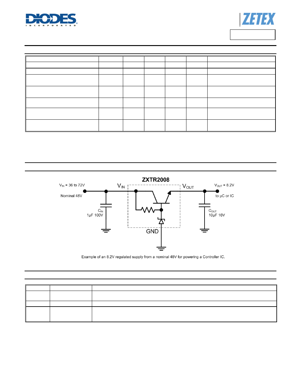
Typical Application Circuit
Pin Functions
Pin Name
Pin Function
Notes
V
IN
Input Supply
To maintain output regulation the input voltage can vary from 12V to 100V with respect to the GND pin. It is
recommended to connect a 1µF capacitor to GND.
GND
Power Ground
This pin should be tied to the system ground.
V
OUT
Voltage Output
Outputs a regulated 8.2V. It is recommended to connect a 10µF capacitor to GND. Minimum of 10µA must
be drawn from V
OUT
to maintain regulation. The pin can be pulled high to a maximum of 14.5V with respect
to ground.