Maximum ratings, Thermal characteristics, Electrical characteristics – Diodes MMDT5401 User Manual
Page 2
MMDT5401
Document Number: DS30169 Rev: 10 - 2
2 of 5
April 2013
© Diodes Incorporated
MMDT5401
ADVAN
CE I
N
F
O
RM
ATI
O
N
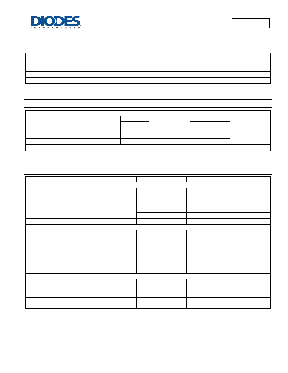
Maximum Ratings
(@T
A
= +25°C, unless otherwise specified.)
Characteristic Symbol
Value
Unit
Collector-Base Voltage
V
CBO
-160 V
Collector-Emitter Voltage
V
CEO
-150 V
Emitter-Base Voltage
V
EBO
-6 V
Continuous Collector Current
I
C
-200 mA
Thermal Characteristics
(@T
A
= +25°C, unless otherwise specified.)
Characteristic Symbol
Value
Unit
Power Dissipation
(Note 5)
P
D
200
mW
(Notes 6 & 7)
320
Thermal Resistance, Junction to Ambient
(Note 5)
R
θJA
625
°C/W
(Notes 6 & 7)
390
Thermal Resistance, Junction to Case
(Note 8)
R
θJC
140
Operating and Storage Temperature Range
T
J
, T
STG
-55 to +150
°C
Electrical Characteristics
(@T
A
= +25°C, unless otherwise specified.)
Characteristic Symbol
Min
Typ
Max
Unit
Test
Condition
OFF CHARACTERISTICS
Collector-Base Breakdown Voltage
BV
CBO
-160
V
I
C
= -100µA, I
E
= 0
Collector-Emitter Breakdown Voltage (Note 9)
BV
CEO
-150
V
I
C
= -1mA, I
B
= 0
Emitter-Base Breakdown Voltage
BV
EBO
-6
V
I
E
= -100µA, I
C
= 0
Collector-Base Cutoff Current
I
CBO
-50 nA
V
CB
= -120V, I
E
= 0
-50 µA
V
CB
= -120V, I
E
= 0, T
A
= +100°C
Base-Emitter Cutoff Current
I
EBO
-50 nA
V
EB
= -5V, I
C
= 0
ON CHARACTERISTICS (Note 9)
DC Current Gain
h
FE
50
I
C
= -1.0mA, V
CE
= -5.0V
60 240
I
C
= -10mA, V
CE
= -5.0V
50
I
C
= -50mA, V
CE
= -5.0V
Collector-Emitter Saturation Voltage
V
CE(sat)
-0.2
V
I
C
= -10mA, I
B
= -1.0mA
-0.5
I
C
= -50mA, I
B
= -5.0mA
Base-Emitter Saturation Voltage
V
BE(sat)
-1.0 V
I
C
= -10mA, I
B
= -1.0mA
I
C
= -50mA, I
B
= -5.0mA
SMALL SIGNAL CHARACTERISTICS
Output Capacitance
C
obo
6.0 pF
V
CB
= -10V, f = 1.0MHz, I
E
= 0
Small Signal Current Gain
h
fe
40
200
I
C
= -1mA, V
CE
= -10V, f = 1.0MHz
Current Gain-Bandwidth Product
f
T
100
300 MHz
I
C
= -10mA, V
CE
= -10V, f = 100MHz
Noise Figure
NF
8.0 dB
V
CE
= -5.0V, I
C
= -200µA,
R
S
= 10Ω
f = 1.0kHz
Notes:
5. For a device mounted on minimum recommended pad layout 1oz weight copper that is on a single-sided FR4 PCB; device is measured under still air
conditions whilst operating in a steady-state.
6. Same as Note 5, except the device is mounted 25mm X 25mm 2oz copper.
7. Maximum combined dissipation.
8. Thermal resistance from junction to the top of package.
9. Measured under pulsed conditions. Pulse width
300µs. Duty cycle 2%.