Electrical characteristics, Mmbt3906fa – Diodes MMBT3906FA User Manual
Page 4
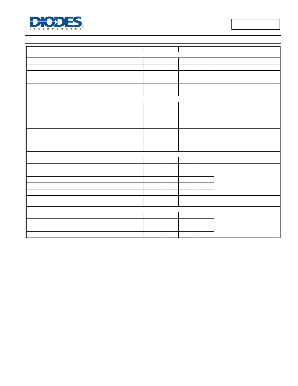
MMBT3906FA
Document number: DS36017 Rev. 1 - 2
4 of 7
July 2013
© Diodes Incorporated
MMBT3906FA
Electrical Characteristics
(@T
A
= +25°C, unless otherwise specified.)
Characteristic Symbol
Min
Max
Unit
Test
Condition
OFF CHARACTERISTICS
Collector-Base Breakdown Voltage
BV
CBO
-40
V
I
C
= -10µA, I
E
= 0
Collector-Emitter Breakdown Voltage (Note 8)
BV
CEO
-40
V
I
C
= -1.0mA, I
B
= 0
Emitter-Base Breakdown Voltage
BV
EBO
-6.0
V
I
E
= -10µA, I
C
= 0
Collector Cutoff Current
I
CEX
-50 nA
V
CE
= -30V, V
EB(OFF)
= -3.0V
Collector Cutoff Current
I
CBO
-50 nA
V
CB
= -30V, I
E
= 0
Base Cutoff Current
I
BL
-50 nA
V
CE
= -30V, V
EB(OFF)
= -3.0V
ON CHARACTERISTICS (Note 8)
DC Current Gain
h
FE
60
80
100
60
30
300
I
C
= -100µA, V
CE
= -1.0V
I
C
= -1.0mA, V
CE
= -1.0V
I
C
= -10mA, V
CE
= -1.0V
I
C
= -50mA, V
CE
= -1.0V
I
C
= -100mA, V
CE
= -1.0V
Collector-Emitter Saturation Voltage
V
CE(sat)
-0.25
-0.40
V
I
C
= -10mA, I
B
= -1.0mA
I
C
= -50mA, I
B
= -5.0mA
Base-Emitter Saturation Voltage
V
BE(sat)
-0.65
-0.85
-0.95
V
I
C
= -10mA, I
B
= -1.0mA
I
C
=- 50mA, I
B
= -5.0mA
SMALL SIGNAL CHARACTERISTICS
Output Capacitance
C
obo
4.5 pF
V
CB
= -5.0V, f = 1.0MHz, I
E
= 0
Input Capacitance
C
ibo
10 pF
V
EB
= -0.5V, f = 1.0MHz, I
C
= 0
Input Impedance
h
ie
2.0 12 k
V
CE
= -10V, I
C
= -1.0mA,
f = 1.0kHz
Voltage Feedback Ratio
h
re
0.1 10
x
10
-4
Small Signal Current Gain
h
fe
100 400
Output Admittance
h
oe
3.0 60 µS
Current Gain-Bandwidth Product
f
T
300
MHz
V
CE
= -20V, I
C
= -10mA,
f = 100MHz
SWITCHING CHARACTERISTICS
Delay Time
t
d
35 ns
V
CC
= -3.0V, I
C
= -10mA,
V
BE(off)
= 0.5V, I
B1
= -1.0mA
Rise Time
t
r
35 ns
Storage Time
t
s
225 ns
V
CC
= -3.0V, I
C
= -10mA,
I
B1
= I
B2
= -1.0mA
Fall Time
t
f
75 ns
Note:
8. Measured under pulsed conditions. Pulse width
300µs. Duty cycle 2%.