Maximum ratings, Thermal characteristics, Mmbt3904lp – Diodes MMBT3904LP User Manual
Page 2
MMBT3904LP
Document number: DS31835 Rev. 4 - 2
2 of 5
October 2011
© Diodes Incorporated
MMBT3904LP
Maximum Ratings
@T
A
= 25°C unless otherwise specified
Characteristic Symbol
Value
Unit
Collector-Base Voltage
V
CBO
60 V
Collector-Emitter Voltage
V
CEO
40 V
Emitter-Base Voltage
V
EBO
6.0 V
Collector Current - Continuous (Note 4)
I
C
200 mA
Thermal Characteristics
Characteristic Symbol
Value
Unit
Power Dissipation (Note 4)
P
D
250 mW
Thermal Resistance, Junction to Ambient (Note 4)
R
θJA
500
°C/W
Operating and Storage and Temperature Range
T
J
, T
STG
-55 to +150
°C
Notes:
4. Device mounted on FR-4 PCB pad layout as shown on Diodes, Inc. suggested pad layout AP02001, which can be found on our website at
1E-06
0.00001
0.0001
0.001
0.01
0.1
1
10
100
1,000
10,000
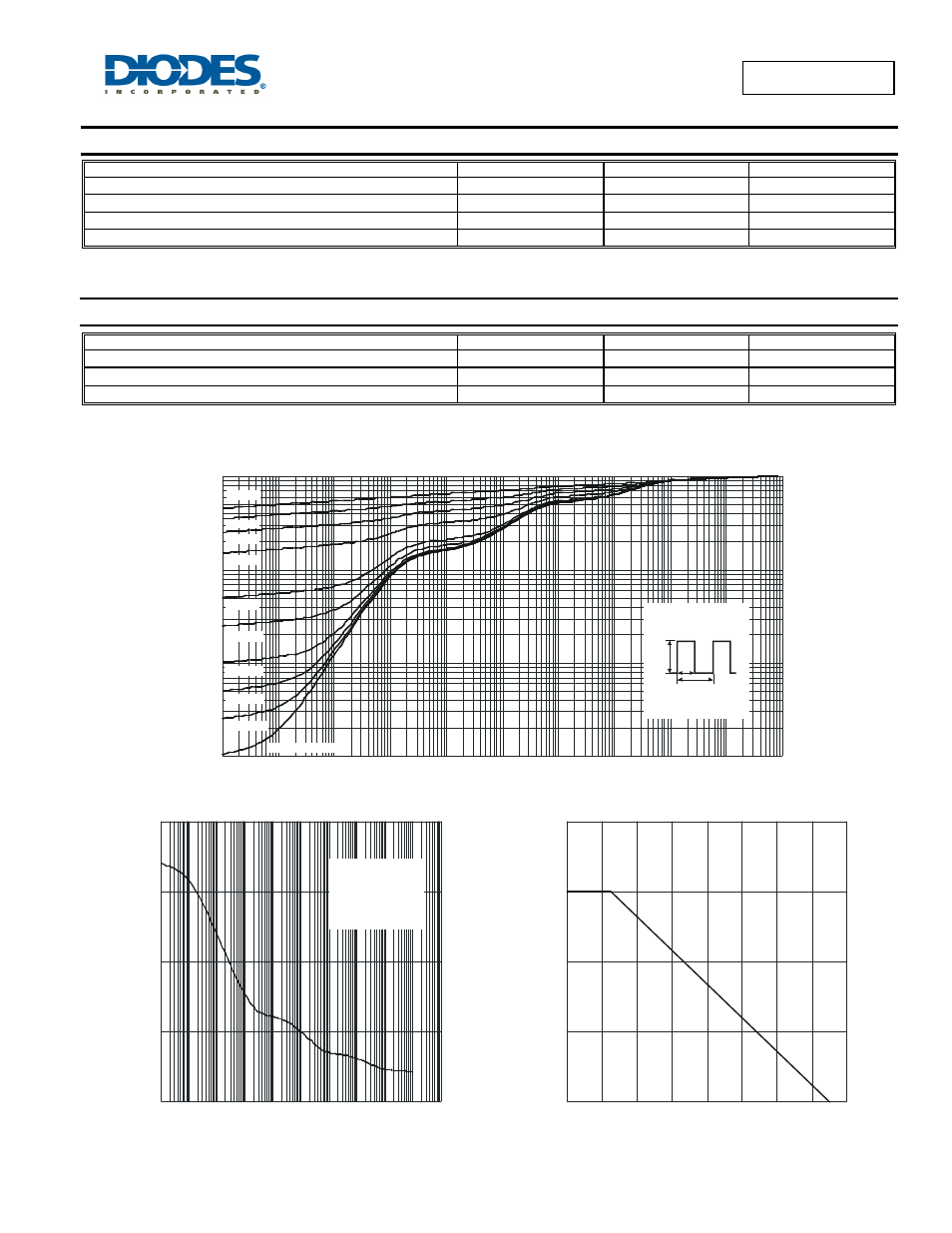
Fig. 1 Transient Thermal Response
t , PULSE DURATION TIME (s)
1
0.001
0.01
0.1
1
r(
t),
T
R
AN
SI
EN
T
T
H
E
R
MA
L
R
ES
IS
T
AN
C
E
T - T = P * R
(t)
Duty Cycle, D = t /t
J
A
JA
1 2
θ
R
(t) = r(t) *
θJA
R
R
= 500°C/W
θ
θ
JA
JA
P(pk)
t
1
t
2
D = 0.7
D = 0.5
D = 0.3
D = 0.05
D = 0.02
D = 0.01
D = 0.005
D = 0.9
D = 0.1
D = Single Pulse
1E-06
0.0001
0.01
1
100
10,000
Fig. 2 Single Pulse Maximum Power Dissipation
t , PULSE DURATION TIME (s)
1
1
10
100
1,000
P
(p
k
),
P
EA
K
T
R
ANSI
EN
T
P
O
WE
R
(W
)
0.1
Single Pulse
T - T = P * R
(t)
J
A
JA
θ
R
(t) = r(t) *
θJA
R
R
= 500°C/W
θ
θ
JA
JA
0
0.1
0.2
0.3
0.4
0
20
40
60
80
100
120
140
160
T , AMBIENT TEMPERATURE ( C)
A
°
Fig. 3 Power Dissipation vs. Ambient Temperature
P
,
P
O
WE
R
DI
SS
IP
A
T
IO
N
(W
)
D
Note 4