Diodes DT1140-04LP User Manual
Features, Mechanical data, Ordering information

DT1140-04LP
Document number: DS36293 Rev. 2 - 2
1 of 5
September 2013
© Diodes Incorporated
DT1140-04LP
ADVAN
CE I
N
F
O
RM
ATI
O
4 CHANNEL LOW CAPACITANCE TVS DIODE ARRAY
Features
Clamping Voltage:9V at 10A 100ns TLP; 9V at 6A 8μs/20μs
IEC 61000-4-2 (ESD): Air – +20/-18kV, Contact – +20/-16kV
IEC 61000-4-5 (Lightning): ±6A (8/20µs)
4 Channels of ESD protection
Low Channel Input Capacitance of 0.5pF Typical
TLP Dynamic Resistance: 0.25Ω
Typically Used for High Speed Ports such as USB 2.0, DVI,
HDMI, Ethernet Port, IEEE,MDDI,PCI Express ,SATA/ eSATA
Totally Lead-Free & Fully RoHS Compliant (Notes 1 & 2)
Halogen and Antimony Free. “Green” Device (Note 3)
Mechanical Data
Case: U-DFN2510-10
Case Material: Molded Plastic, “Green” Molding Compound
UL Flammability Classification Rating 94V-0
Moisture Sensitivity: Level 1 per J-STD-020
Terminals: NiPdAu over Copper leadframe (Lead Free Plating)
Solderable per MIL-STD-202, Method 208
Weight: 0.038 grams (approximate)
Ordering Information
(Note 4)
Product
Compliance Marking
Reel Size (inches)
Tape Width (mm)
Quantity per Reel
DT1140-04LP-7
Standard
BC2
7
8
3,000/Tape & Reel
Notes:
1. No purposely added lead. Fully EU Directive 2002/95/EC (RoHS) & 2011/65/EU (RoHS 2) compliant.
2. S more information about Diodes Incorporated’s definitions of Halogen- and Antimony-free, "Green"
and Lead-free.
3. Halogen- and Antimony-free "Green” products are defined as those which contain <900ppm bromine, <900ppm chlorine (<1500ppm total Br + Cl) and
<1000ppm antimony compounds.
4. For packaging details, go to our website at
Marking Information
Date Code Key
Year
2013
2014
2015
2016 2017 2018
Code A
B
C
D
E
F
Month
Jan
Feb
Mar
Apr
May
Jun
Jul
Aug
Sep
Oct
Nov
Dec
Code 1 2 3 4 5 6 7 8 9 O N D
Pin #
Description
1, 2, 4, 5
I/O
6, 7, 9, 10
No Connection
3, 8
Vss
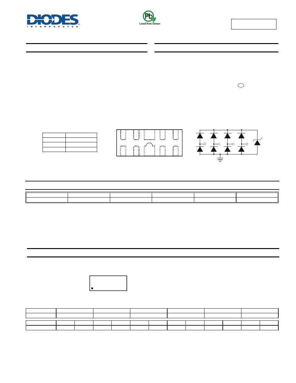
Pin Description (Top View)
Device Schematic
BC2 = Product Type Marking Code
YM = Date Code Marking
Y = Year (ex: A = 2013)
M = Month (ex: 9 = September)
1
2
3
4
5
10
9
8
7
6
Pin 1
Pin 2
3,8
Pin 5
Pin 4
TF2
YM
BC2
e4
