Diodes DMF05LCFLP User Manual
Dmf05lcflp new prod uc t, Features, Mechanical data
DMF05LCFLP
Document number: DS32004 Rev. 3 - 2
1 of 4
July 2010
© Diodes Incorporated
DMF05LCFLP
NEW PROD
UC
T
FIVE ELEMENT COMMON ANODE ESD-PROTECTION DIODE ARRAY
Features
•
5-line ESD Protection
•
Sub-miniature Package (1.6 x 1.6mm)
•
Low Capacitance – 42pF typ @ V
R
= 0V
•
Provides a High Level of Protection from ESD to IEC61000-4-2
•
±30kV Contact Discharge
•
±30kV Air Discharge
•
Lead Free/RoHS Compliant (Note 1)
•
"Green" Device (Note 2)
•
Qualified to AEC-Q101 Standards for High Reliability
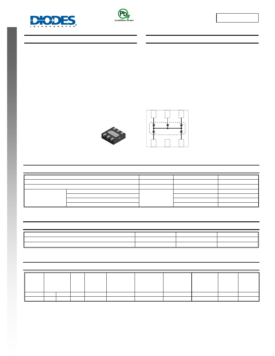
Mechanical Data
• Case:
DFN1616-6
•
Case Material: Molded Plastic, “Green” Molding Compound.
UL Flammability Classification Rating 94V-0
•
Moisture Sensitivity: Level 1 per J-STD-020
•
Terminals: Solderable per MIL-STD-202, Method 208
•
Lead Free Plating (NiPdAu Finish over Copper leadframe).
•
Polarity: Pin 1 Dot and Center Pad Notch, See Diagram
•
Marking Information: See Page 2
•
Ordering Information: See Page 2
•
Weight: 0.004 grams (approximate)
Maximum Ratings
@T
A
= 25°C unless otherwise specified
Characteristic Symbol
Value
Unit
Peak Pulse Current, 8/20
μs waveform, single shot, per IEC61000-4-5
I
PPM
5 A
Peak Pulse Power, 8/20
μs waveform, single shot, per IEC61000-4-5
P
PP
70 W
ESD Rating
Human Body Model
ESD
8 kV
Machine Model
400
V
IEC61000-4-2 Air Discharge
30
kV
IEC61000-4-2 Contact Discharge
30
kV
Thermal Characteristics
Characteristic Symbol
Value
Unit
Thermal Resistance Junction to Ambient Air (Note 3)
R
θJA
256
°C/W
Operating and Storage Temperature Range
T
J
, T
STG
-55 to +150
°C
Electrical Characteristics
@T
A
= 25°C unless otherwise specified
Reverse
Standoff
Voltage
V
RWM
@
I
RWM
= 1
μA
Breakdown
Voltage
V
BR
@ I
T
Test
Current
Max. Reverse
Leakage @
V
RWM
(Note 4)
Max. Clamping
Voltage
@ I
PP
= 1A
per IEC61000-4-5
Max. Clamping
Voltage V
c
@ I
PP
= 5A
per IEC61000-4-5
Max. Forward
Clamping
Voltage V
F
@ I
F
= 1A
per IEC61000-4-5
Max. Forward
Clamping
Voltage V
F
@ I
F
= 5A
per IEC61000-4-5
Max Total
Capacitance
V
R
= 0V
f = 1MHz
Typical Total
Capacitance
V
R
= 2.5V
f = 1MHz
Min (V)
Min (V) Max (V) I
T
(mA)
I
R
(
μA) V
C
(V) V
C
(V)
V
F
(V)
V
F
(V)
C
T
(pF) C
T
(pF)
5.0 6 8 1.0 0.1
9.5
12.5
2
4
50
25
Notes:
1. No Purposefully added Lead.
2. Diodes Inc.'s "Green" policy can be found on our webs3. Part mounted on FR-4 PC board with recommended pad layout, which can be found on our website at Only one switching diode powered on.
4. Short duration pulse test used to minimize self-heating effect.
DFN1616-6
Internal Schematic
TOP VIEW
BOTTOM VIEW
1
2
3
6
5
4