Maximum ratings, Thermal characteristics, Electrical characteristics – Diodes DESDA5V3L User Manual
Page 2
DESDA5V3L
Document number: DS35528 Rev. 3 - 2
2 of 5
January 2013
© Diodes Incorporated
DESDA5V3L
ADVAN
CE I
N
F
O
RM
ATI
O
N
Maximum Ratings
(@T
A
= +25°C, unless otherwise specified.)
Characteristic Symbol
Value
Unit
Conditions
Peak Pulse Power Dissipation
P
PP
300 W
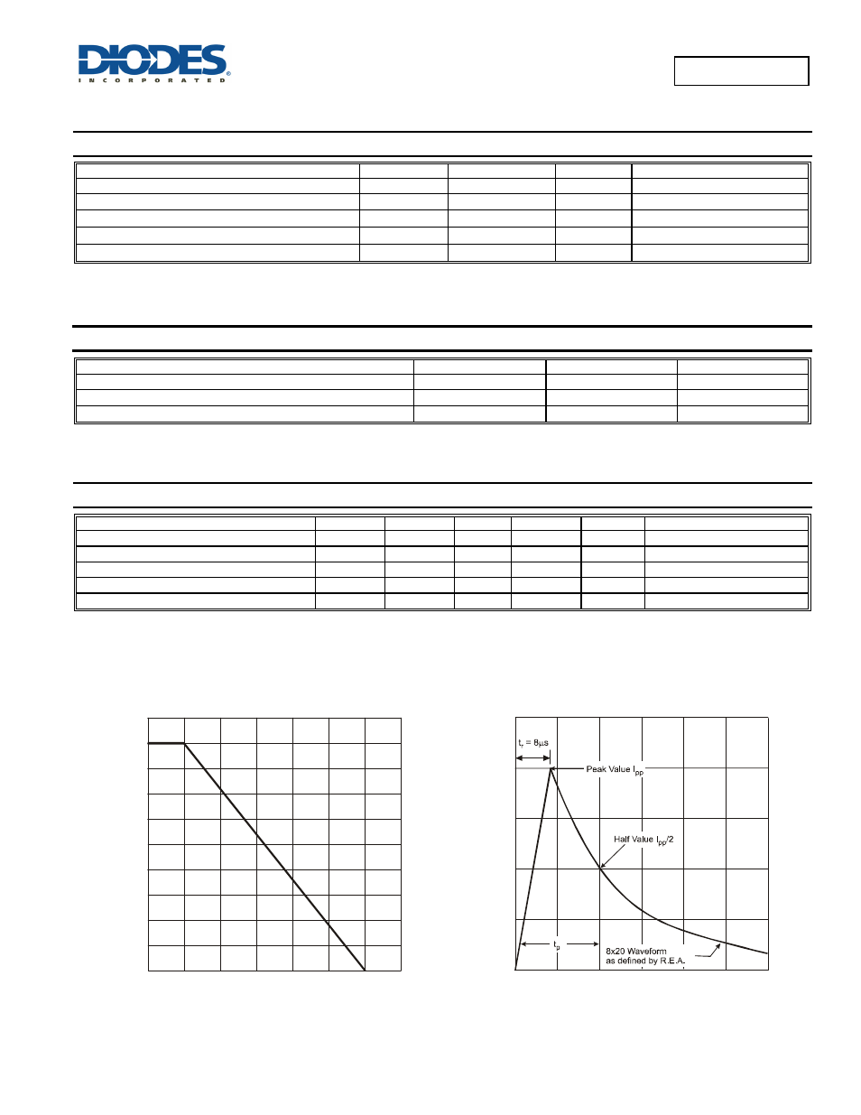
8/20μs, Fig 2
Peak Pulse Current
I
PP
20 A
8/20μs, Fig 2
ESD Protection – Contact Discharge
V
ESD_Contact
±9 kV
Standard
IEC
61000-4-2
ESD Protection – Air Discharge
V
ESD_Air
±16 kV
Standard
IEC
61000-4-2
ESD Protection – Human Body Model
V
HBM
±25
kV
MIL STD 883C – Method 3015-6
Thermal Characteristics
Characteristic Symbol
Value
Unit
Power Dissipation (Note 5)
P
D
250 mW
Thermal Resistance, Junction to Ambient (Note 5)
R
θJA
500
°C/W
Operating and Storage Temperature Range
T
J
, T
STG
-55 to +150
°C
Electrical Characteristics
(@T
A
= +25°C, unless otherwise specified.)
Characteristic
Symbol
Min
Typ
Max
Unit
Test Conditions
Reverse Breakdown Voltage
V
BR
5.3
−
5.9 V
I
R
= 1mA
Reverse Current (Note 6)
I
RM
−
−
2
μA
V
RM
= 3V
Forward Voltage
V
F
−
−
1.25 V
I
F
= 200mA
Dynamic Resistance
R
D
−
0.28
−
Ω
I
pp
= 15A, tp = 2.5μs
Channel Input Capacitance
C
IN
−
−
220 pF
V
IN
= 0V, f = 1MHz
Notes:
5. Device mounted on FR-4 PCB pad layout (2oz copper) as shown on Diodes, Inc. suggested pad layout AP02001, which can be found on our website at
6. Short duration pulse test used to minimize self-heating effect.
0
125
175
150
50
100
0
T , AMBIENT TEMPERATURE ( C)
Figure 1 Power Derating Curve
A
°
P
,
P
O
WE
R
DIS
S
IP
A
T
IO
N (
m
W
)
D
25
100
50
75
150
25
75
125
300
175
Note 5
250
200
0
t, TIME ( s)
Figure 2 Typical 8 x 20µs Pulse Waveform
μ
20
40
60
100
50
0
I
, PE
AK P
U
LS
E
C
URRENT
(
%
I
)
Pp
p
P