Diodes DMG4712SSS User Manual
Dmg4712sss new prod uc t, Features, Mechanical data
DMG4712SSS
Document number: DS32040 Rev. 6 - 2
1 of 6
August 2010
© Diodes Incorporated
DMG4712SSS
NEW PROD
UC
T
N-CHANNEL ENHANCEMENT MODE MOSFET WITH SCHOTTKY DIODE
Features
•
High Density UMOS with Schottky Barrier Diode
•
Low Leakage Current at High Temperature
• High
Conversion
Efficiency
• Low
On-Resistance
•
Low Input Capacitance
•
Fast Switching Speed
•
Utilizes Diodes’ Monolithic DIOFET Technology to Increase
Conversion Efficiency
•
UIS Tested, R
G
Tested
•
Lead Free By Design/RoHS Compliant (Note 1)
•
"Green" Device (Note 2)
•
Qualified to AEC-Q101 Standards for High Reliability
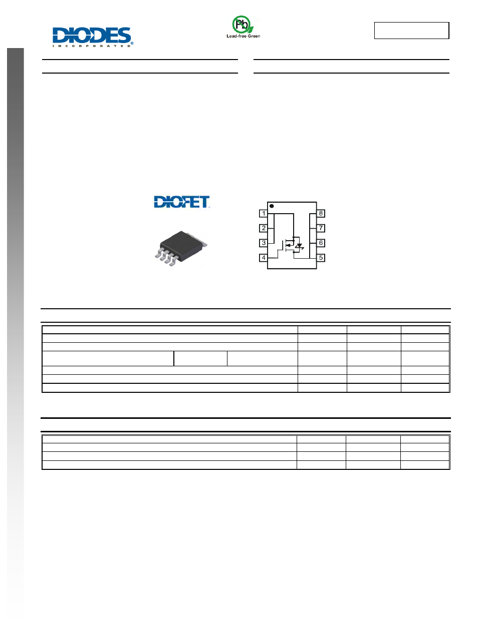
Mechanical Data
• Case:
SO-8
•
Case Material: Molded Plastic, “Green” Molding Compound.
UL Flammability Classification Rating 94V-0
•
Moisture Sensitivity: Level 1 per J-STD-020
•
Terminal Connections: See Diagram Below
•
Marking Information: See Page 5
•
Ordering Information: See Page 5
•
Weight: 0.072 grams (approximate)
Maximum Ratings
@T
A
= 25°C unless otherwise specified
Characteristic
Symbol
Value
Unit
Drain-Source Voltage
V
DSS
30 V
Gate-Source Voltage
V
GSS
±12 V
Continuous Drain Current (Note 3)
Steady
State
T
A
= 25°C
T
A
= 85°C
I
D
11.2
6.6
A
Pulsed Drain Current (Note 4)
I
DM
63 A
Avalanche Current (Notes 4 & 5)
I
AR
30 A
Repetitive Avalanche Energy (Notes 4 & 5) L = 0.1mH
E
AR
45 mJ
Thermal Characteristics
Characteristic Symbol
Value
Unit
Power Dissipation (Note 3)
P
D
1.55 W
Thermal Resistance, Junction to Ambient @T
A
= 25°C (Note 3)
R
θJA
81.3 °C/W
Operating and Storage Temperature Range
T
J
,
T
STG
-55 to +150
°C
Notes:
1. No purposefully added lead.
2. Diodes Inc.'s "Green" policy can be found on our webs 3. Device mounted on FR-4 PCB with minimum recommended pad layout. The value in any given application depends on the user’s specific board design.
4. Repetitive rating, pulse width limited by junction temperature.
5.
I
AR
and E
AR
rating are based on low frequency and duty cycles to keep T
J
= 25°C. L = 0.1mH, V
DD
= 0V, R
G
= 0
Ω, rated V
DS
= 30V, and V
GS
= 10V.
Top View
Top View
Internal Schematic
S
D
D
G
D
D
S
S
D
iodes Schottky
I
ntegrated M
O
S
FET