Dmc6070lfdh advanced information, Maximum ratings q1 n-channel, Maximum ratings q2 p-channel – Diodes DMC6070LFDH User Manual
Page 2: Thermal characteristics, Dmc6070lfdh
POWERDI is a registered trademark of Diodes Incorporated.
DMC6070LFDH
Document number: DS36083 Rev. 6 - 2
2 of 10
November 2013
© Diodes Incorporated
DMC6070LFDH
ADVANCED INFORMATION
Maximum Ratings Q1 N-CHANNEL
(@T
A
= +25°C, unless otherwise specified.)
Characteristic Symbol
Value
Units
Drain-Source Voltage
V
DSS
60 V
Gate-Source Voltage
V
GSS
±20 V
Continuous Drain Current (Note 5) V
GS
= 10V
Steady
State
T
A
= +25°C
T
A
= +70°C
I
D
3.1
2.5
A
t<10s
T
A
= +25°C
T
A
= +70°C
I
D
3.9
3.1
A
Maximum Body Diode Forward Current (Note 5)
I
S
2 A
Pulsed Drain Current (10μs pulse, Duty cycle = 1%)
I
DM
15 A
Maximum Ratings Q2 P-CHANNEL
(@T
A
= +25°C, unless otherwise specified.)
Characteristic Symbol
Value
Units
Drain-Source Voltage
V
DSS
-60 V
Gate-Source Voltage
V
GSS
±20 V
Continuous Drain Current (Note 5) V
GS
= -10V
Steady
State
T
A
= +25°C
T
A
= +70°C
I
D
-2.4
-1.9
A
t<10s
T
A
= +25°C
T
A
= +70°C
I
D
-2.9
-2.3
A
Maximum Body Diode Forward Current (Note 5)
I
S
-2 A
Pulsed Drain Current (10μs pulse, Duty cycle = 1%)
I
DM
-12 A
Thermal Characteristics
(@T
A
= +25°C, unless otherwise specified.)
Characteristic Symbol
Value
Units
Total Power Dissipation (Note 5)
P
D
1.4 W
Thermal Resistance, Junction to Ambient (Note 5)
Steady state
R
θJA
91
°C/W
t<10s 60
Thermal Resistance, Junction to Case (Note 5)
R
θJC
32
Operating and Storage Temperature Range
T
J,
T
STG
-55 to +150
°C
Note:
5. Device mounted on FR-4 substrate PC board, 2oz copper, with thermal bias to bottom layer 1inch square copper plate
0.00001
0.0001
0.001
0.01
0.1
1
10
100
1,000
t1, PULSE DURATION TIME (sec)
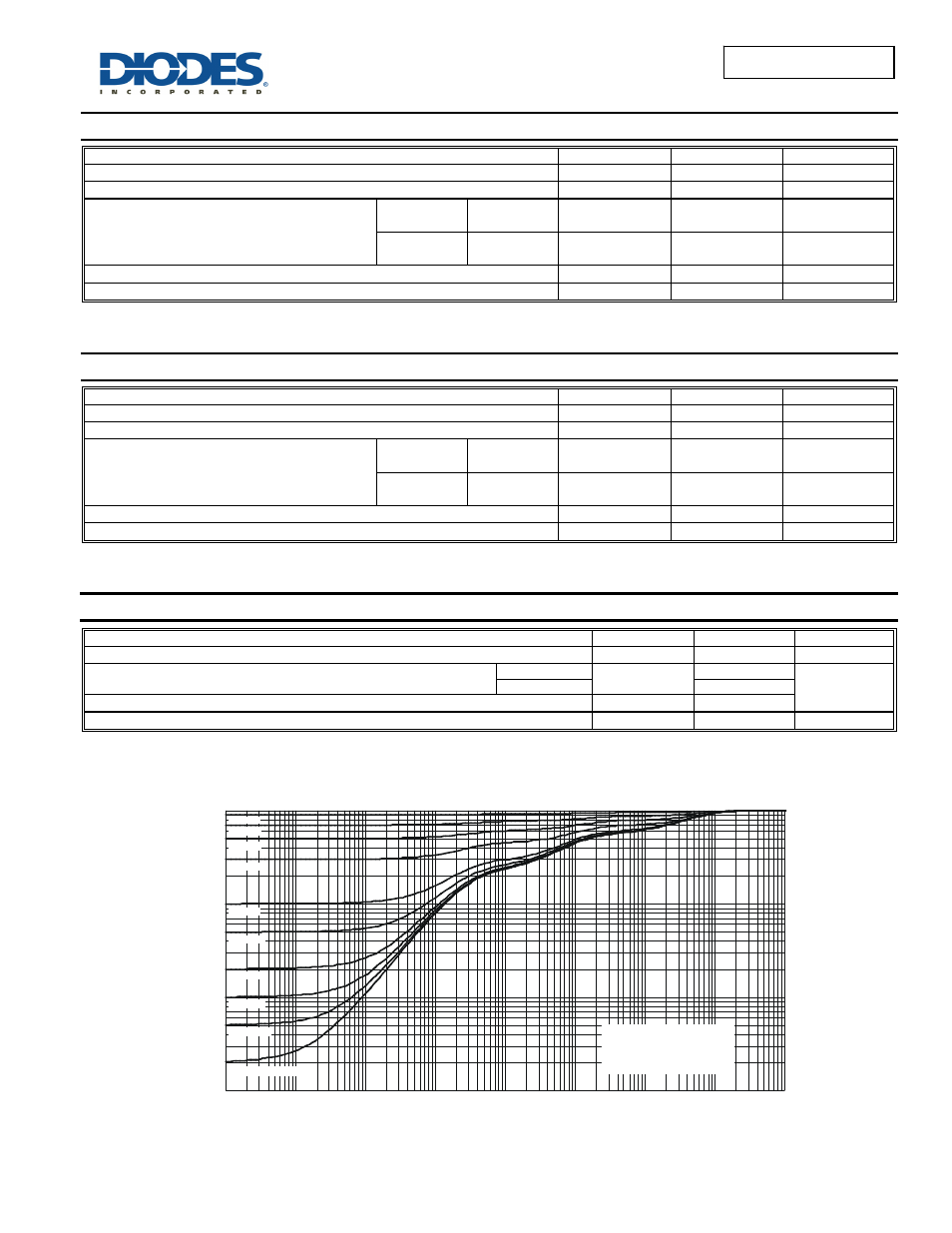
Figure 1 Transient Thermal Resistance
R
(t) = r(t) * R
R
= 116°C/W
Duty Cycle, D = t1/ t2
JA
JA
JA
0.001
r(t),
T
R
ANSI
E
N
T
T
H
E
R
MA
L
R
ES
IS
TAN
C
E
0.01
0.1
1
D = 0.5
D = 0.7
D = 0.9
D = 0.3
D = 0.1
D = 0.05
D = 0.02
D = 0.01
D = 0.005
D = Single Pulse