Diodes DMC6040SSD User Manual
Product summary, Description and applications, Features and benefits
DMC6040SSD
Document number: DS36829 Rev. 1 - 2
1 of 9
June 2014
© Diodes Incorporated
DMC6040SSD
ADVAN
CE I
N
F
O
RM
ATI
O
N
NEW PROD
UC
T
COMPLEMENTARY PAIR ENHANCEMENT MODE MOSFET
Product Summary
Device
V
(BR)DSS
R
DS(on) max
I
D
T
A
= +25°C
Q1
N-Channel
60V
40m
Ω @ V
GS
= 10V
6.5 A
55m
Ω @ V
GS
= 4.5V
5.6 A
Q2
P-Channel
-60V
110m
Ω @ V
GS
= -10V
-3.9 A
130m
Ω @ V
GS
= -4.5V
-3.6 A
Description and Applications
This new generation MOSFET has been designed to minimize the on-
state resistance (R
DS(ON)
) and yet maintain superior switching
performance, making it ideal for high efficiency power management
applications.
• DC-DC
Converters
•
Power Management Functions
• Backlighting
Features and Benefits
•
Low Input Capacitance
• Low
On-Resistance
•
Fast Switching Speed
•
Totally Lead-Free & Fully RoHS Compliant (Notes 1 & 2)
•
Halogen and Antimony Free. “Green” Device (Note 3)
•
Qualified to AEC-Q101 Standards for High Reliability
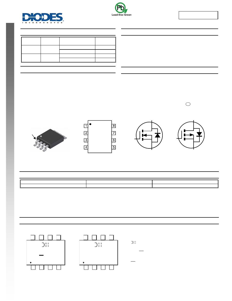
Mechanical Data
• Case:
SO-8
•
Case Material: Molded Plastic, “Green” Molding Compound.
UL Flammability Classification Rating 94V-0
•
Moisture Sensitivity: Level 1 per J-STD-020
•
Terminal Connections: See Diagram
•
Terminals: Finish – Tin Finish annealed over Copper leadframe.
Solderable per MIL-STD-202, Method 208
•
Weight: 0.074 grams (approximate)
Ordering Information
(Note 4)
Part Number
Case
Packaging
DMC6040SSD-13
SO-8
2,500/Tape & Reel
Notes:
1. No purposely added lead. Fully EU Directive 2002/95/EC (RoHS) & 2011/65/EU (RoHS 2) compliant.
2. S more information about Diodes Incorporated’s definitions of Halogen- and Antimony-free, "Green"
and Lead-free.
3. Halogen- and Antimony-free "Green” products are defined as those which contain <900ppm bromine, <900ppm chlorine (<1500ppm total Br + Cl) and
<1000ppm antimony compounds.
4. For packaging details, go to our website at
Marking Information
= Manufacturer’s Marking
C6040SD = Product Type Marking Code
YYWW = Date Code Marking
YY or YY = Year (ex: 14= 2014)
WW = Week (01 - 53)
YY = Date Code Marking for SAT (Shanghai Assembly/ Test site)
YY = Date Code Marking for CAT (Chengdu Assembly/ Test site)
Chengdu A/T Site
Shanghai A/T Site
1
4
8
5
C6040SD
WW
YY
1
4
8
5
C6040SD
WW
YY
Top View
SO-8
Top View
Pin Configuration
D1
S1
G1
D2
S2
G
2
Q1 N-Channel MOSFET
Q2 P-Channel MOSFET
S1
D2
S2
D1
G2
G1
D1
D2
Pin1
e3