Diodes DMP58D0SV User Manual
Features, Mechanical data, Maximum ratings
DMP58D0SV
Document number: DS31293 Rev. 4 - 2
1 of 5
www.diodes.com
July 2009
© Diodes Incorporated
DMP58D0SV
DUAL P-CHANNEL ENHANCEMENT MODE FIELD EFFECT TRANSISTOR
Features
• Low
On-Resistance
•
ESD Protected Gate to 500V
•
Low Input Capacitance
•
Fast Switching Speed
•
Lead Free By Design/RoHS Compliant (Note 3)
•
“Green” Device (Note 4)
•
Qualified to AEC-Q 101 Standards for High Reliability
Mechanical Data
• Case:
SOT-563
•
Case Material: Molded Plastic, "Green" Molding Compound.
UL Flammability Classification Rating 94V-0
•
Moisture Sensitivity: Level 1 per J-STD-020D
• Terminals:
Finish
⎯ Matte Tin annealed over Copper leadframe.
Solderable per MIL-STD-202, Method 208
•
Terminal Connections: See Diagram
•
Marking Information: See Page 3
•
Ordering Information: See Page 3
•
Weight: 0.006 grams (approximate)
Maximum Ratings
@T
A
= 25°C unless otherwise specified
Characteristic Symbol
Value
Units
Drain-Source Voltage
V
DSS
-50 V
Drain-Gate Voltage (Note 1)
V
DGR
-50 V
Gate-Source Voltage
Continuous
V
GSS
±20
V
Drain Current (Note 2)
Continuous
I
D
-160 mA
Thermal Characteristics
@T
A
= 25°C unless otherwise specified
Characteristic Symbol
Value
Units
Total Power Dissipation (Note 2)
P
D
400 mW
Thermal Resistance, Junction to Ambient (Note 2)
R
θJA
313
°C/W
Operating and Storage Temperature Range
T
J
, T
STG
-55 to +150
°C
Electrical Characteristics
@T
A
= 25°C unless otherwise specified
Characteristic Symbol
Min
Typ
Max
Unit
Test
Condition
OFF CHARACTERISTICS (Note 5)
Drain-Source Breakdown Voltage
BV
DSS
-50
⎯
⎯
V
V
GS
= 0V, I
D
= -250
μA
Zero Gate Voltage Drain Current
I
DSS
⎯
⎯
-1
μA V
DS
= -50V, V
GS
= 0V
Gate-Body Leakage
I
GSS
⎯
⎯
±5
μA V
GS
=
±20V, V
DS
= 0V
ON CHARACTERISTICS (Note 5)
Gate Threshold Voltage
V
GS(th)
-0.8
⎯
-2.1
V
V
DS
= V
GS
, I
D
= -250
μA
Static Drain-Source On-Resistance
R
DS (ON)
⎯
6 8
Ω V
GS
= -5V, I
D
= -0.100A
Forward Transconductance
g
FS
0.05
⎯
⎯
S
V
DS
= -25V, I
D
= -0.1A
DYNAMIC CHARACTERISTICS
Input Capacitance
C
iss
⎯
27
⎯
pF
V
DS
= -25V, V
GS
= 0V, f = 1.0MHz
Output Capacitance
C
oss
⎯
4
⎯
pF
Reverse Transfer Capacitance
C
rss
⎯
1.4
⎯
pF
Notes:
1. R
GS
≤ 20KΩ.
2. Device mounted on FR-4 PCB, 1 inch x 0.85 inch x 0.062 inch; pad layout as shown on Diodes Inc. suggested pad layout document AP02001, which
can be found on our website3. No purposefully added lead.
4. Diodes Inc’s “Green” policy can be found on our websit5. Short duration pulse test used to minimize self-heating effect.
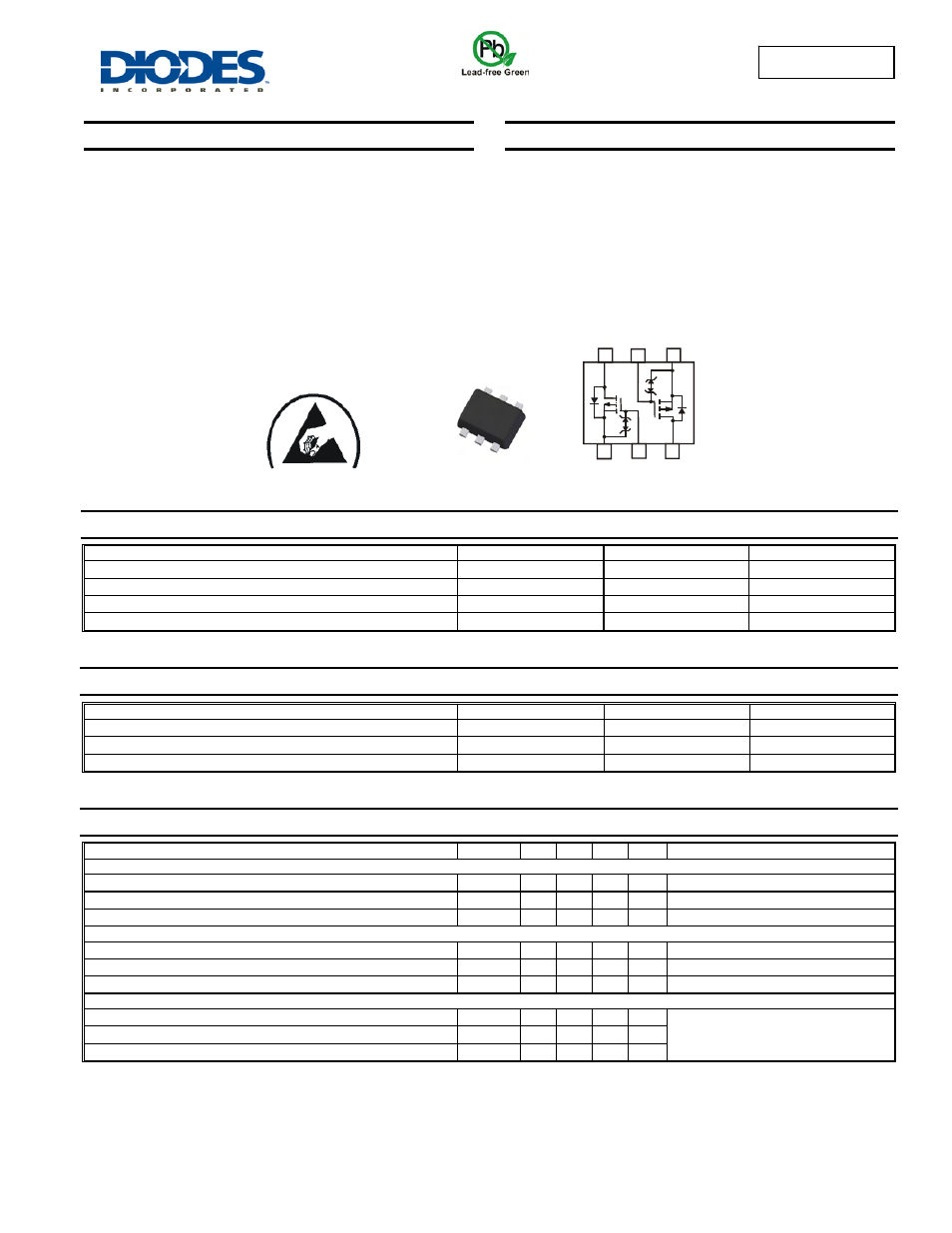
SOT-563
TOP VIEW
Internal Schematic
TOP VIEW
S
1
D
1
D
2
S
2
G
1
G
2
ESD protected to 500V