Diodes DMP3030SN User Manual
Dmp3030sn new prod uc t, Features, Mechanical data
DMP3030SN
Document number: DS30787 Rev. 5 - 2
1 of 4
August 2011
© Diodes Incorporated
DMP3030SN
NEW PROD
UC
T
P-CHANNEL ENHANCEMENT MODE FIELD EFFECT TRANSISTOR
Features
• Low
On-Resistance
•
Low Gate Threshold Voltage
•
Low Input Capacitance
•
Fast Switching Speed
•
Lead Free By Design/RoHS Compliant (Note 2)
•
ESD Protected Gate
•
"Green" Device (Note 4)
•
Qualified to AEC-Q101 standards for High Reliability
Mechanical Data
• Case:
SC59
•
Case Material: Molded Plastic, “Green” Molding
Compound. UL Flammability Classification Rating 94V-0
•
Moisture sensitivity: Level 1 per J-STD-020C
• Terminals:
Finish
⎯ Matte Tin annealed over Copper
leadframe. Solderable per MIL-STD-202, Method 208
•
Terminal Connections: See Diagram
•
Marking Information: See Page 3
•
Ordering & Date Code Information: See Page 3
•
Weight: 0.014 grams (approximate)
Maximum Ratings
@T
A
= 25°C unless otherwise specified
Characteristic
Symbol
Value
Unit
Drain-Source Voltage
V
DSS
-30
V
Gate-Source Voltage
V
GSS
±20
V
Drain Current (Note 1) Steady State
I
D
-0.7
A
Pulsed Drain Current (Note 3)
I
DM
-2.8
A
Thermal Characteristics
@T
A
= 25°C unless otherwise specified
Characteristic
Symbol
Value
Unit
Total Power Dissipation (Note 1)
P
d
500
mW
Thermal Resistance, Junction to Ambient
R
θJA
250
°C/W
Operating and Storage Temperature Range
T
j
, T
STG
-65 to +150
°C
Electrical Characteristics
@T
A
= 25°C unless otherwise specified
Characteristic
Symbol
Min
Typ
Max
Unit
Test Condition
OFF CHARACTERISTICS (Note 5)
Drain-Source Breakdown Voltage
BV
DSS
-30
⎯
⎯
V
V
GS
= 0V, I
D
= -250µA
Zero Gate Voltage Drain Current
I
DSS
⎯
⎯
-10
μA V
DS
= -30V, V
GS
= 0V
Gate-Body Leakage
I
GSS
⎯
⎯
±10
μA V
GS
=
±20V, V
DS
= 0V
ON CHARACTERISTICS (Note 5)
Gate Threshold Voltage
V
GS(th)
-1.0
⎯
-3.0
V
V
DS
= -10V, I
D
= -1.0mA
Static Drain-Source On-Resistance
R
DS (ON)
⎯
0.20
0.35
0.25
0.45
Ω
V
GS
= -10V, I
D
= -0.4A
V
GS
= -4.5V, I
D
= -0.4A
Forward Transfer Admittance
|Y
fs
|
⎯
1
⎯
S
V
DS
= -10V, I
D
= -0.4A
Diode Forward Voltage (Note 5)
V
SD
⎯
-0.8
-1.1
V
V
GS
= 0V, I
S
= -0.7A
DYNAMIC CHARACTERISTICS
Input Capacitance
C
iss
⎯
160
⎯
pF
V
DS
= -10V, V
GS
= 0V
f
= 1.0MHz
Output Capacitance
C
oss
⎯
120
⎯
pF
Reverse Transfer Capacitance
C
rss
⎯
50
⎯
pF
SWITCHING CHARACTERISTICS
Turn-On Delay Time
t
D(ON)
⎯
10
⎯
ns
V
DD
= -10V, I
D
= -0.4A,
V
GS
= -5.0V, R
GEN
= 50
Ω
Turn-Off Delay Time
t
D(OFF)
⎯
25
⎯
ns
Turn-On Rise Time
t
r
⎯
25
⎯
ns
Turn-Off Fall Time
t
f
⎯
40
⎯
ns
Notes:
1. Device mounted on FR-4 PCB.
2. No purposefully added lead.
3. Pulse width
≤10μS, Duty Cycle ≤1%.
4. Diodes Inc.'s "Green" policy can be found on our websit
5. Short duration pulse test used to minimize self-heating effect.
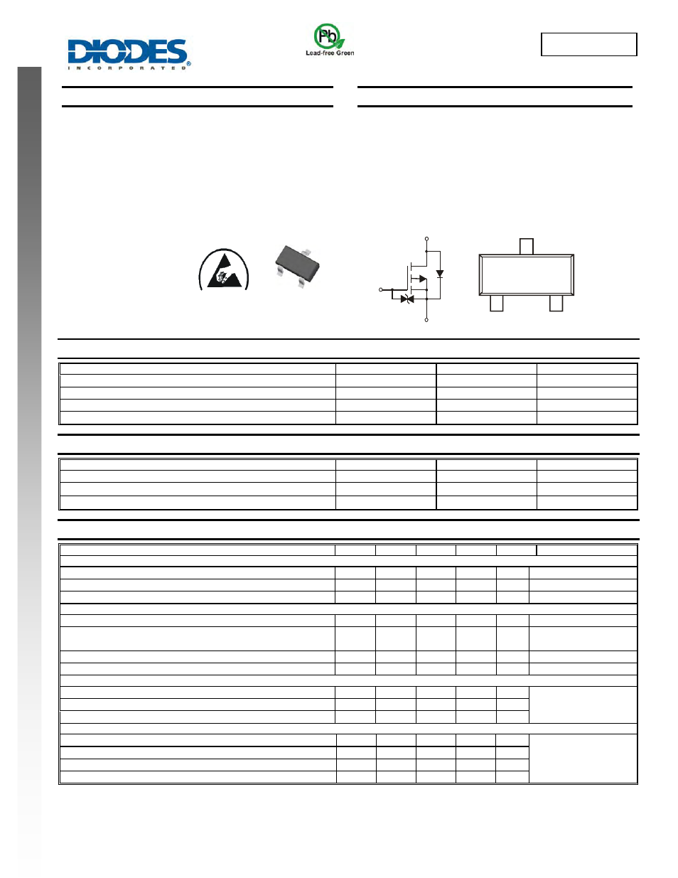
SC59
TOP VIEW
Internal Schematic
ESD protected
Source
EQUIVALENT CIRCUIT
Gate
Protection
Diode
Gate
Drain
D
G
S