Electrical characteristics, Dmp2305uvt, A product line of diodes incorporated – Diodes DMP2305UVT User Manual
Page 4
DMP2305UVT
Document number: DS35986 Rev. 1 - 2
4 of 8
August 2012
© Diodes Incorporated
A Product Line of
Diodes Incorporated
DMP2305UVT
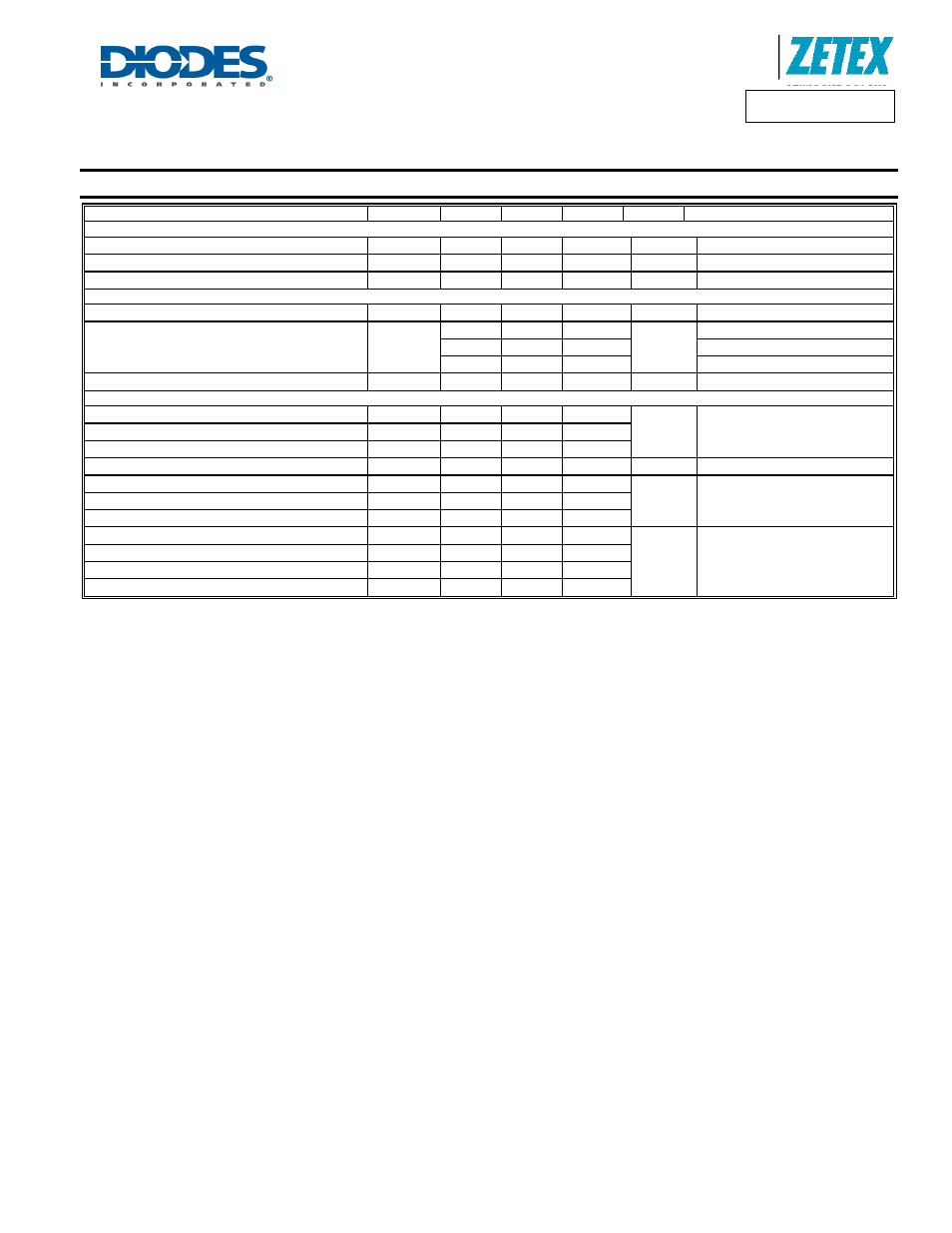
Electrical Characteristics
@T
A
= 25°C unless otherwise specified
Characteristic Symbol
Min
Typ
Max
Unit
Test
Condition
OFF CHARACTERISTICS (Note 7)
Drain-Source Breakdown Voltage
BV
DSS
-20
⎯
⎯
V
V
GS
= 0V, I
D
= -250
μA
Zero Gate Voltage Drain Current
I
DSS
⎯
⎯
-1 µA
V
DS
= -20V, V
GS
= 0V
Gate-Source Leakage
I
GSS
⎯
⎯
±100
nA
V
GS
=
±8V, V
DS
= 0V
ON CHARACTERISTICS (Note 7)
Gate Threshold Voltage
V
GS(th)
-0.5
⎯
-0.9 V
V
DS
= V
GS
, I
D
= -250
μA
Static Drain-Source On-Resistance
R
DS (ON)
⎯
45 60
m
Ω
V
GS
= -4.5V, I
D
= -4.2A
⎯
60 90
V
GS
= -2.5V, I
D
= -3.4A
⎯
87 113
V
GS
= -1.8V, I
D
= -2.0A
Forward Transfer Admittance
|Y
fs
|
⎯
9
⎯
S
V
DS
= -5V, I
D
= -4A
DYNAMIC CHARACTERISTICS (Note 8)
Input Capacitance
C
iss
⎯
727
⎯
pF
V
DS
= -20V, V
GS
= 0V
f = 1.0MHz
Output Capacitance
C
oss
⎯
69
⎯
Reverse Transfer Capacitance
C
rss
⎯
64
⎯
Gate Resistance
R
G
⎯
23
⎯
Ω
V
GS
= 0V, V
DS
= 0V, f = 1.0MHz
Total Gate Charge
Q
g
⎯
7.6
⎯
nC
V
GS
= -4.5V, V
DS
= -4V, I
D
= -3.5A
Gate-Source Charge
Q
gs
⎯
1.4
⎯
Gate-Drain Charge
Q
gd
⎯
1.2
⎯
Turn-On Delay Time
t
D(on)
⎯
14.0
⎯
ns
V
DS
= -4V, V
GS
= -4.5V,
R
L
= 4
Ω, R
G
= 6
Ω, I
D
= -1A
Turn-On Rise Time
t
r
⎯
13.0
⎯
Turn-Off Delay Time
t
D(off)
⎯
53.8
⎯
Turn-Off Fall Time
t
f
⎯
23.2
⎯
Notes:
7. Short duration pulse test used to minimize self-heating effect.
8. Guaranteed by design. Not subject to product testing.