Diodes DMP2240UDM User Manual
Features, Mechanical data, Maximum ratings
DMP2240UDM
Document number: DS31197 Rev. 5 - 2
1 of 5
April 2010
© Diodes Incorporated
DMP2240UDM
DUAL P-CHANNEL ENHANCEMENT MODE FIELD EFFECT TRANSISTOR
Features
•
Dual P-Channel MOSFET
• Low
On-Resistance
• 150
m
Ω @ V
GS
= -4.5V
• 200
m
Ω @ V
GS
= -2.5V
• 240
m
Ω @ V
GS
= -1.8V
•
Very Low Gate Threshold Voltage V
GS(th)
≤ 1V
•
Low Input Capacitance
•
Fast Switching Speed
•
Low Input/Output Leakage
•
Lead Free By Design/RoHS Compliant (Note 2)
•
"Green" Device (Note 3)
•
Qualified to AEC-Q101 standards for High Reliability
Mechanical Data
• Case:
SOT-26
•
Case Material: Molded Plastic, “Green” Molding Compound.
UL Flammability Classification Rating 94V-0
•
Moisture Sensitivity: Level 1 per J-STD-020
•
Terminals Connections: See Diagram
• Terminals:
Finish
⎯ Matte Tin annealed over Copper leadframe.
Solderable per MIL-STD-202, Method 208
•
Marking Information: See Page 4
•
Ordering Information: See Page 4
•
Weight: 0.015 grams (approximate)
Maximum Ratings
@T
A
= 25°C unless otherwise specified
Characteristic Symbol
Value
Units
Drain-Source Voltage
V
DSS
-20 V
Gate-Source Voltage
V
GSS
±12 V
Drain Current (Note 1)
T
A
= 25
°C
T
A
= 70
°C
I
D
-2.0
-1.5
A
Pulsed Drain Current
I
DM
-7 A
Thermal Characteristics
Characteristic Symbol
Value
Units
Total Power Dissipation (Note 1)
P
D
600 mW
Thermal Resistance, Junction to Ambient
R
θJA
208 °C/W
Operating and Storage Temperature Range
T
J,
T
STG
-65 to +150
°C
Notes:
1. Device mounted on FR-4 PCB.
2. No purposefully added lead.
3. Diodes Inc.’s “Green” policy can be found on our webs
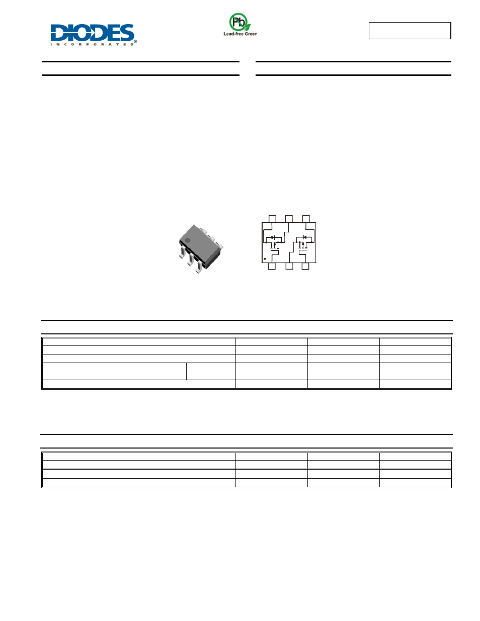
SOT-26
TOP VIEW
TOP VIEW
Internal Schematic
S
1
D
1
D
2
S
2
G
1
G
2
1
2
3
4
5
6
G1
S2
G2
D2
S1
D1