Dmp2123l new prod uc t, Maximum ratings, Thermal characteristics – Diodes DMP2123L User Manual
Page 2: Electrical characteristics, Dmp2123l
DMP2123L
Document number: DS31440 Rev. 2 - 2
2 of 5
October 2013
© Diodes Incorporated
DMP2123L
NEW PROD
UC
T
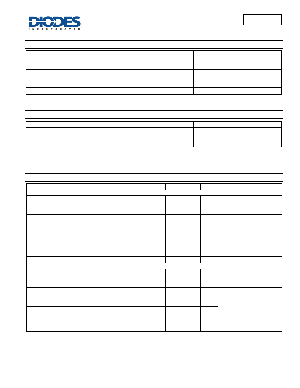
Maximum Ratings
(@T
A
= +25°C, unless otherwise specified.)
Characteristic Symbol
Value
Unit
Drain-Source Voltage
V
DSS
-20 V
Gate-Source Voltage
V
GSS
12
V
Drain Current (Note 5) Continuous
T
A
= +25°C
T
A
= +70°C
I
D
-3.0
-2.4
A
Pulsed Drain Current (Note 6)
I
DM
-15 A
Body-Diode Continuous Current (Note 5)
I
S
2.0 A
Thermal Characteristics
Characteristic Symbol
Value
Unit
Total Power Dissipation (Note 5)
P
D
1.4 W
Thermal Resistance, Junction to Ambient (Note 5); Steady-State
R
θJA
90
C/W
Operating and Storage Temperature Range
T
J
, T
STG
-55 to +150
C
Notes:
5. Device mounted on 1"x1", FR-4 PC board with 2 oz. Copper and test pulse width t
10s.
6. Repetitive Rating, pulse width limited by junction temperature.
Electrical Characteristics
(@T
A
= +25°C, unless otherwise specified.)
Characteristic Symbol
Min
Typ
Max
Unit
Test
Condition
STATIC PARAMETERS
Drain-Source Breakdown Voltage
BV
DSS
-20
V
I
D
= -250µA, V
GS
= 0V
Zero Gate Voltage Drain Current T
J
= +25°C
I
DSS
-1 µA
V
DS
= -20V, V
GS
= 0V
Gate-Body Leakage Current
I
GSS
100
nA
V
DS
= 0V, V
GS
=
12V
Gate Threshold Voltage
V
GS(th)
-0.6
-1.25 V
V
DS
= V
GS
, I
D
= -250µA
On State Drain Current (Note 7)
I
D (ON)
-15
A
V
GS
= -4.5V, V
DS
= -5V
Static Drain-Source On-Resistance (Note 7)
R
DS(ON)
51
87
99
72
108
123
m
V
GS
= -4.5V, I
D
= -3.5A
V
GS
= -2.7V, I
D
= -3.0A
V
GS
= -2.5V, I
D
= -2.6A
Forward Transconductance (Note 7)
g
FS
7.3
S
V
DS
= -10V, I
D
= -3.0A
Diode Forward Voltage (Note 5)
V
SD
0.79 -1.26 V I
S
= -1.7A, V
GS
= 0V
Maximum Body-Diode Continuous Current (Note 5)
I
S
1.7 A
DYNAMIC PARAMETERS (Note 8)
Total Gate Charge
Q
g
7.3
nC
V
GS
= -4.5V, V
DS
= -10V, I
D
= -3.0A
Gate-Source Charge
Q
gs
2.0
nC
V
GS
= -4.5V, V
DS
= -10V, I
D
= -3.0A
Gate-Drain Charge
Q
gd
1.9
nC
V
GS
= -4.5V, V
DS
= -10V, I
D
= -3.0A
Turn-On Delay Time
t
D(on)
12
ns
V
DS
= -10V, V
GS
= -4.5V,
R
L
= 10
, R
G
= 6
Turn-On Rise Time
t
r
20
ns
Turn-Off Delay Time
t
D(off)
38
ns
Turn-Off Fall Time
t
f
41
ns
Input Capacitance
C
iss
443
pF
V
DS
= -16V, V
GS
= 0V
f = 1.0MHz
Output Capacitance
C
oss
128
pF
Reverse Transfer Capacitance
C
rss
101
pF
Notes:
7. Test pulse width t = 300µs.
8. Guaranteed by design. Not subject to production testing.