Maximum ratings, Thermal characteristics, Electrical characteristics – Diodes DMP2104V User Manual
Page 2: Dmp2104v
DMP2104V
Document number: DS30942 Rev. 7 - 2
2 of 6
March 2011
© Diodes Incorporated
DMP2104V
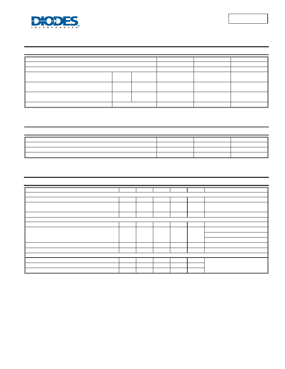
Maximum Ratings
@T
A
= 25°C unless otherwise specified
Characteristic Symbol
Value
Units
Drain-Source Voltage
V
DSS
-20 V
Gate-Source Voltage
V
GSS
±12 V
Continuous Drain Current (Note 4) V
GS
= -4.5V
Steady
State
T
A
= 25°C
T
A
= 70°C
I
D
-1.9
-1.5
A
Continuous Drain Current (Note 4) V
GS
= -4.5V
t
≤ 5s
T
A
= 25°C
T
A
= 70°C
I
D
-2.1
-1.65
A
Continuous Drain Current (Note 4) V
GS
= -2.5V
Steady
State
T
A
= 25°C
T
A
= 70°C
I
D
-1.7
-1.3
A
Pulsed Drain Current
t
p
= 10
μs I
DM
-4.0 A
Thermal Characteristics
Characteristic Symbol
Value
Units
Power Dissipation (Note 4)
P
D
0.85 W
Thermal Resistance, Junction to Ambient @T
A
= 25°C (Note 4)
R
θJA
146 °C/W
Operating and Storage Temperature Range
T
J,
T
STG
-55 to +150
°C
Electrical Characteristics
@T
A
= 25°C unless otherwise specified
Characteristic Symbol
Min
Typ
Max
Unit
Test
Condition
OFF CHARACTERISTICS (Note 5)
Drain-Source Breakdown Voltage
BV
DSS
-20
⎯
⎯
V
V
GS
= 0V, I
D
= -250
μA
Zero Gate Voltage Drain Current T
J
= 25
°C
T
J
= 125
°C
I
DSS
⎯
⎯
-1.0
-5.0
μA
V
DS
= -20V, V
GS
= 0V
Gate-Source Leakage
I
GSS
⎯
⎯
±100
nA
V
GS
=
±12V, V
DS
= 0V
ON CHARACTERISTICS (Note 5)
Gate Threshold Voltage
V
GS(th)
-0.45
⎯
-1.0 V
V
DS
= V
GS
, I
D
= -250
μA
Static Drain-Source On-Resistance
R
DS (ON)
⎯
92
134
180
150
200
240
m
Ω
V
GS
= -4.5V, I
D
= -950mA
V
GS
= -2.5V, I
D
= -670mA
V
GS
= -1.8V, I
D
= -200mA
Forward Transconductance
g
FS
⎯
3.1
⎯
S
V
DS
= -10V, I
D
= -810mA
Diode Forward Voltage (Note 5)
V
SD
⎯
⎯
-0.9 V
V
GS
= 0V, I
S
= -360mA
DYNAMIC CHARACTERISTICS
Input Capacitance
C
iss
⎯
320
⎯
pF
V
DS
= -16V, V
GS
= 0V
f = 1.0MHz
Output Capacitance
C
oss
⎯
80
⎯
pF
Reverse Transfer Capacitance
C
rss
⎯
60
⎯
pF
Notes:
4. Device mounted on FR-4 PCB with 1 inch square pads.
5. Short duration pulse test used to minimize self-heating effect.