Maximum ratings, Thermal characteristics, Electrical characteristics – Diodes DMP2004TK User Manual
Page 2: Dmp2004tk
DMP2004TK
Document number: DS30932 Rev. 5 - 2
2 of 5
August 2012
© Diodes Incorporated
DMP2004TK
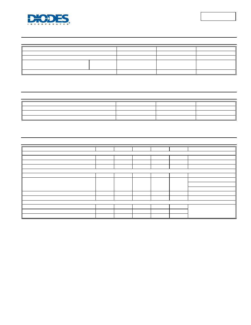
Maximum Ratings
(@T
A
= +25°C, unless otherwise specified.)
Characteristic Symbol
Value
Units
Drain-Source Voltage
V
DSS
-20 V
Gate-Source Voltage
V
GSS
±8 V
Drain Current (Note 5)
Steady
State
T
A
= +25
°C
T
A
= +85
°C
I
D
-430
-310
mA
Pulsed Drain Current (Note 6)
I
DM
-750 mA
Thermal Characteristics
(@T
A
= +25°C, unless otherwise specified.)
Characteristic Symbol
Value
Units
Total Power Dissipation (Note 5)
P
D
150 mW
Thermal Resistance, Junction to Ambient
R
θJA
833 °C/W
Operating and Storage Temperature Range
T
J,
T
STG
-55 to +150
°C
Electrical Characteristics
(@T
A
= +25°C, unless otherwise specified.)
Characteristic Symbol
Min
Typ
Max
Unit
Test
Condition
OFF CHARACTERISTICS (Note 7)
Drain-Source Breakdown Voltage
BV
DSS
-20
⎯
⎯
V
V
GS
= 0V, I
D
= -250
μA
Zero Gate Voltage Drain Current
I
DSS
⎯
⎯
-1.0
μA
V
DS
= -20V, V
GS
= 0V
Gate-Source Leakage
I
GSS
⎯
⎯
±1.0
μA
V
GS
=
±4.5V, V
DS
= 0V
ON CHARACTERISTICS (Note 7)
Gate Threshold Voltage
V
GS(th)
-0.5
⎯
-1.0 V
V
DS
= V
GS
, I
D
= -250
μA
Static Drain-Source On-Resistance
R
DS (ON)
⎯
0.7
1.1
1.7
1.1
1.6
2.4
Ω
V
GS
= -4.5V, I
D
= -430mA
V
GS
= -2.5V, I
D
= -300mA
V
GS
= -1.8V, I
D
= -150mA
Forward Transfer Admittance
|Y
fs
|
200
⎯
⎯
ms
V
DS
=10V, I
D
= 0.2A
Diode Forward Voltage (Note 7)
V
SD
⎯
⎯
-1.4 V
V
GS
= 0V, I
S
= -115mA
DYNAMIC CHARACTERISTICS
Input Capacitance
C
iss
⎯
⎯
175 pF
V
DS
= -16V, V
GS
= 0V
f = 1.0MHz
Output Capacitance
C
oss
⎯
⎯
30 pF
Reverse Transfer Capacitance
C
rss
⎯
⎯
20 pF
Notes:
5. Device mounted on FR-4 PCB.
6. Pulse width
≤10μS, Duty Cycle ≤1%
7. Short duration pulse test used to minimize self-heating effect.